Holistic lithography for EUV - Brion Technologies, Inc.
Holistic lithography for EUV - Brion Technologies, Inc.
Holistic lithography for EUV - Brion Technologies, Inc.
- No tags were found...

You also want an ePaper? Increase the reach of your titles
YUMPU automatically turns print PDFs into web optimized ePapers that Google loves.
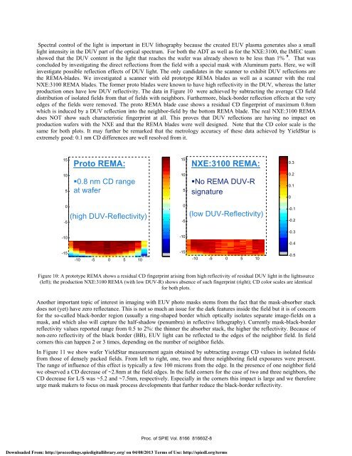
Spectral control of the light is important in <strong>EUV</strong> <strong>lithography</strong> because the created <strong>EUV</strong> plasma generates also a small<br />
light intensity in the DUV part of the optical spectrum. For both the ADT as well as <strong>for</strong> the NXE:3100, the IMEC team<br />
showed that the DUV content in the light that reaches the wafer was already shown to be less than 1% 9 . That was<br />
concluded by investigating the direct reflections from the field with a special mask with Aluminum parts. Here, we will<br />
investigate possible reflection effects of DUV light. The only candidates in the scanner to exhibit DUV reflections are<br />
the REMA-blades. We investigated a scanner with old prototype REMA blades as well as a scanner with the real<br />
NXE:3100 REMA blades. The <strong>for</strong>mer proto blades were known to have high reflectivity in the DUV, whereas the latter<br />
production ones have low DUV reflectivity. The data in Figure 10 were achieved by subtracting the average CD field<br />
distribution of isolated fields from that of fields with neighbors. Furthermore, black-border reflection effects at the very<br />
edges of the fields were removed. The proto REMA blade case shows a residual CD fingerprint of maximum 0.8nm<br />
which is induced by a DUV reflection into the neighbor-field by the bottom REMA blade. The real NXE:3100 REMA<br />
does NOT show such characteristic fingerprint at all. This proves that DUV reflections are having no impact on<br />
production wafers with the NXE and that the REMA blades were well designed. Note that the CD color scale is the<br />
same <strong>for</strong> both plots. It may further be remarked that the metrology accuracy of these data achieved by YieldStar is<br />
extremely good: 0.1 nm CD differences are well resolved from it.<br />
15<br />
Proto REMA:<br />
0.3<br />
15<br />
NXE:3100 REMA:<br />
0.3<br />
10<br />
5<br />
•0.8 nm CD range<br />
at wafer<br />
0.2<br />
0.1<br />
0.0<br />
10<br />
5<br />
•No REMA DUV-R<br />
signature<br />
0.2<br />
0.1<br />
0<br />
0<br />
-5<br />
(high DUV-Reflectivity)<br />
-0.1<br />
-0.2<br />
0<br />
-5<br />
(low DUV-Reflectivity)<br />
-0.1<br />
-0.2<br />
-10<br />
-0.3<br />
-10<br />
-0.4<br />
-0.3<br />
-0.4<br />
-15<br />
-10 -5 0 5 10<br />
-0.5<br />
-15<br />
-10 -5 0 5 10<br />
-0.5<br />
Figure 10: A prototype REMA shows a residual CD fingerprint arising from high reflectivity of residual DUV light in the lightsource<br />
(left); the production NXE:3100 REMA (with low DUV-R) shows absence of such fingerprint (right); CD color scales are identical<br />
<strong>for</strong> both plots.<br />
Another important topic of interest in imaging with <strong>EUV</strong> photo masks stems from the fact that the mask-absorber stack<br />
does not (yet) have zero reflectance. This is not so much an issue <strong>for</strong> the dark features inside the field but it is of concern<br />
<strong>for</strong> the so-called black-border region (usually a ring-shaped border which optically isolates separate image-fields on a<br />
mask, and which also will capture the half-shadow (penumbra) in reflective <strong>lithography</strong>). Currently mask-black-border<br />
reflectivity values reported range from 0.5 to 2%: the thinner the absorber stack, the higher the reflectivity. Because of<br />
non-zero reflectivity of the black border (BB), <strong>EUV</strong> light can be reflected to the edges of the neighbor field. In field<br />
corners this can happen 2 or 3 times, depending on the number of neighbor fields.<br />
In Figure 11 we show wafer YieldStar measurement again obtained by subtracting average CD values in isolated fields<br />
from those of densely packed fields. From left to right, one, two and three neighboring field exposures were present.<br />
The range of influence of this effect is typically a few 100 microns from the edge. In the presence of one neighbor field<br />
we observed a CD decrease of ~2.8nm at the field edges. In the field corners <strong>for</strong> the case of two and three neighbors, the<br />
CD decrease <strong>for</strong> L/S was ~5.2 and ~7.5nm, respectively. Especially in the corners this impact is large and we there<strong>for</strong>e<br />
urge mask makers to focus on mask process developments that further reduce the black-border reflectivity.<br />
Proc. of SPIE Vol. 8166 81660Z-8<br />
Downloaded From: http://proceedings.spiedigitallibrary.org/ on 04/08/2013 Terms of Use: http://spiedl.org/terms