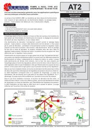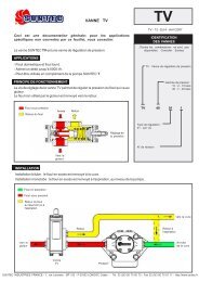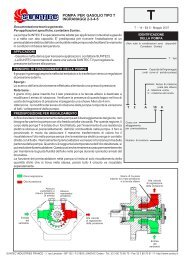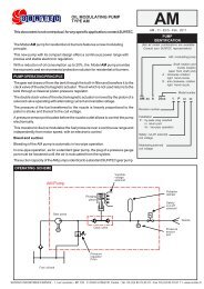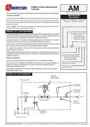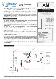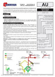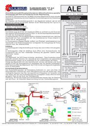
suntec xpress
suntec xpress
suntec xpress

You also want an ePaper? Increase the reach of your titles
YUMPU automatically turns print PDFs into web optimized ePapers that Google loves.
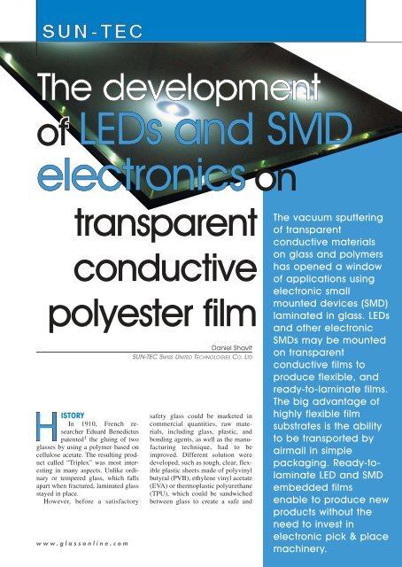
of<br />
transparent<br />
conductive<br />
polyester film<br />
ISTORY<br />
In 1910, French researcher<br />
Eduard Benedictus<br />
patented 1 the gluing of two<br />
glasses by using a polymer based on<br />
cellulose acetate. The resulting product<br />
called “Triplex” was most interesting<br />
in many aspects. Unlike ordinary<br />
or tempered glass, which falls<br />
apart when fractured, laminated glass<br />
stayed in place.<br />
However, before a satisfactory<br />
www.glassonline.com<br />
Daniel Shavit<br />
SUN-TEC SWISS UNITED TECHNOLOGIES CO.LTD<br />
safety glass could be marketed in<br />
commercial quantities, raw materials,<br />
including glass, plastic, and<br />
bonding agents, as well as the manufacturing<br />
technique, had to be<br />
improved. Different solution were<br />
developed, such as tough, clear, flexible<br />
plastic sheets made of polyvinyl<br />
butyral (PVB), ethylene vinyl acetate<br />
(EVA) or thermoplastic polyurethane<br />
(TPU), which could be sandwiched<br />
between glass to create a safe and<br />
on<br />
The vacuum sputtering<br />
of transparent<br />
conductive materials<br />
on glass and polymers<br />
has opened a window<br />
of applications using<br />
electronic small<br />
mounted devices (SMD)<br />
laminated in glass. LEDs<br />
and other electronic<br />
SMDs may be mounted<br />
on transparent<br />
conductive films to<br />
produce flexible, and<br />
ready-to-laminate films.<br />
The big advantage of<br />
highly flexible film<br />
substrates is the ability<br />
to be transported by<br />
airmail in simple<br />
packaging. Ready-tolaminate<br />
LED and SMD<br />
embedded films<br />
enable to produce new<br />
products without the<br />
need to invest in<br />
electronic pick & place<br />
machinery.
Fig. 1 - Typical specification<br />
of laminated glass using<br />
LED embedded films<br />
breakproof material. Today, laminated<br />
glass helps keep the building<br />
envelope intact, reduces the danger<br />
of glass shards, and helps prevent<br />
people from falling through sudden<br />
openings. Users of laminated glass<br />
soon discovered that it also helped<br />
reduce noise, block harmful UV rays<br />
and protect against break-ins. In cars<br />
and in buildings, the use of laminated<br />
glass continues to grow, increasing<br />
safety worldwide.<br />
Fig. 3 - Table. PVB laminated<br />
by Glas Trösch, Switzerland.<br />
Powered @ 48 VDC, 20 mA<br />
In 1877, Prof. A. W. Wright 2 of<br />
Yale University published a paper in<br />
the American Journal of Science and<br />
Arts on the use of an “electrical deposition<br />
apparatus” to form mirrors and<br />
study their properties. There still is<br />
some confusion as whether Wright<br />
was using sputtering or gaseous arcing.<br />
But there is no doubt that this<br />
early research anticipated later<br />
developments, including cathode<br />
shielding, multi-layer coatings, substrate<br />
motion, and hybrid processing.<br />
The applications of vacuum coatings<br />
progressed from the simple single<br />
layer coatings on plates in the 1930s<br />
and 1940s to coatings on flexible<br />
materials in the 1950s. This research<br />
anticipated the energy crises in the<br />
1970s proving the need for energy<br />
conservation coatings on large areas<br />
of glass and polymer webs. As published<br />
in Patents of Ford Motors<br />
(1989) 3 and Saint-Gobain (1990) 4 ,<br />
the use of transparent high conductive<br />
layers on glass was a quite<br />
important solution for pure heating<br />
applications. But since the 1980s<br />
companies such as Sharp KK5<br />
(1983) started to mount small electronic<br />
devices (SMDs) such as LEDs<br />
on transparent conductive glass or<br />
films. The patterning of transparent<br />
conductive layers was carried out by<br />
Fig. 2 - Transparent powered<br />
LED stair containing LED film<br />
from SUN-TEC. EVA type lamination<br />
by Sofraver, Switzerland. Powered<br />
@ 24 VDC, 20 mA per glass<br />
laser 6,7 or by wet etching technology<br />
8,9 . While Matsushita Electric<br />
Ind. 10 would claim in 1983 the<br />
encapsulation by vacuum pressure<br />
bonding using PVB, Fuji Electric<br />
Co 11 and Nippon Sheet Glass 12<br />
would widen the technique to the use<br />
of Silicon and EVA. Beside this<br />
modern sheet type of lamination<br />
companies such as Stanley Electric<br />
Co 13 continued the development of<br />
34 - VACUUM INTERNATIONAL 1/2007 www.glassonline.com
Figure 4<br />
Figure 5<br />
resin lamination based on<br />
Epoxy. Since 1990 (Ricoh<br />
KK 14 and Stanley Electric 15 ) produced<br />
complete LED-Displays combining<br />
IC chips, liquid crystals and<br />
LEDs powered by transparent conductive<br />
layers.<br />
Despite newer patents (examples<br />
16,17,18 ), the main technological<br />
questions regarding the mounting of<br />
SMD elements on patterned transparent<br />
conductive glass and its lamination<br />
was obviously well developed<br />
before 1990.<br />
The disadvantage to transport<br />
heavy glasses from pure glass metallizing<br />
companies to electronic mounting<br />
sites and to forward these heavy<br />
weight flat half-fabricated SMD<br />
mounted glasses to glass lamination<br />
units has driven companies to develop<br />
low weight SMD embedded films,<br />
which may be transported by air-mail<br />
as rolled material.<br />
CURRENT MATERIALS<br />
For the past three years, SUN-<br />
TEC’s SMD- and LED-embedded<br />
films have been processed by wellknown<br />
glass laminating companies<br />
to produce transparent powered ele-<br />
www.glassonline.com<br />
ments. The typical<br />
specification of the laminated<br />
glass, as shown in Figure 1, is<br />
completely air free and it may be<br />
used for indoor as well as humid outdoor<br />
environment.<br />
The use of transparent polymers<br />
such as TPU, EVA or PVB in combination<br />
with vacuum or autoclaving<br />
technology enable the glass industry<br />
to produce standard elements as well<br />
as customer designs with respect to<br />
size or functionality. Stairs, windows<br />
and tables might need less than 20<br />
LEDs per sheet, resulting in currents<br />
below 100 mA.<br />
As shown in Figure 4, it is possible<br />
that transparent conductive oxides on<br />
polyester film may power quite a high<br />
quantity of SMD LEDs without significant<br />
heat production within the<br />
glass laminates. This is due to the fact,<br />
that SMD-LEDs are powered with<br />
less than 20 mA @ 3.5 V per LED.<br />
Fig. 4<br />
52 cm x 36<br />
cm film with 345<br />
LEDs (1843 LEDs/m2 )<br />
PVB type lamination by Glas<br />
Troesch, Switzerland. Current:<br />
60 mA at 48 VDC<br />
Fig. 5 - Floor plate of 50 x 50 cm,<br />
PVB lamination, Glas Troesch,<br />
Switzerland<br />
With a current maximum size of<br />
3,500 x 1,250 millimetres, the transparent<br />
conductive layer, as well as the<br />
connection between the films and the<br />
SMD/LED elements, have to withstand<br />
rolled packaging (current diameter<br />
16 centimetres) and transport,<br />
rough daily handling as well as high<br />
sheer strength at maximum lamination<br />
temperatures of 125°C. As shown<br />
in Figure 6, LED and SMD embedded<br />
films may be laminated together with<br />
additional layers between the glass.<br />
As shown in Figure 7, SUN-TEC<br />
delivers customer designs with<br />
respect to size, geometry and placement<br />
of the LEDs. These designs are<br />
usually sent by e-mail as AutoCAD<br />
file (DWG, DXF).<br />
SUMMARY AND FUTURE<br />
DEVELOPMENTS<br />
The vacuum sputtered transparent<br />
conductive materials on glass and<br />
VACUUM INTERNATIONAL 1/2007 - 35
polymers have opened a wide window<br />
of applications using electronic small<br />
mounted devices (SMD) laminated<br />
between glass, PMME or polycarbonate.<br />
LEDs and other electronic SMD<br />
may be mounted on transparent conductive<br />
films to produce flexible, and<br />
ready to laminate films. The big<br />
advantage of highly flexible film substrates<br />
is the ability to be transported<br />
by fast and low weight airmail in a<br />
simple cylindrical packaging paperboard<br />
with 16 centimetres diameter.<br />
Furthermore, ready to laminate LED<br />
and SMD embedded films enable<br />
glass laminating companies to produce<br />
own new products without the<br />
need to invest in electronic pick &<br />
place machinery.<br />
Further ongoing developments are:<br />
- separately controlled full colour<br />
RGB LEDs for media walls;<br />
- high power LEDs;<br />
Fig. 7 - 325 LEDs for LOGO<br />
“Reflections” before lamination<br />
- Infra Red sensorial SMD elements<br />
in glass (Figure 8);<br />
- film for transparent heating applications;<br />
and<br />
- transparent conductive films for<br />
electromagnetic induction sensors.<br />
REFERENCES<br />
1 Benedictus, Eduard, French<br />
Patent 405,881<br />
2 A.W. Wright, “On the Production<br />
of transparent Metallic Films by<br />
Electrical Discharge in Exhausted<br />
Tubes”, Am. J. Sci. Arts, Vol 13,<br />
pp. 49-55 (1877)<br />
3 US4844985; 1989-07-04; Ford<br />
Motor Co. (US)<br />
4 EP0353142; 1990-01-31; Saint-<br />
Gobain Vitrage (FR)<br />
5 JP58218179; 1983-12-19; Sharp<br />
KK<br />
6 JP60120577; 1985-06-28;<br />
Handotai Energy Kenkyusho<br />
7 DE19854899; 1999-12-30;<br />
Siemens AG (DE)<br />
8 JP63272095; 1988-11-09; Tobi<br />
Co. Ltd.<br />
9 JP1151237; 1989-06-14;<br />
Mitsubishi Electric Corp.<br />
10 JP58137266; 1983-08-15;<br />
Matsushita Electric Ind. Co. Ltd.<br />
11 JP58052884; 1983-03-29; Fuji<br />
Electric Co. Ltd.<br />
Fig. 8 - Use of IR sensitive SMD<br />
elements for sensorial applications<br />
Fig. 6 - EVA stair<br />
laminated by Romag, UK<br />
12 JP60095959; 1985-05-29; Nippon<br />
Sheet Glass Co. Ltd.<br />
13 JP3290982; 1991-12-20; Stanley<br />
Electric Co. Ltd.<br />
14 JP2010395; 1990-01-16; Ricoh<br />
KK; Stanley Electric Co. Ltd.<br />
15 JP5119706; 1993-05-18; Stanley<br />
Electric Co. Ltd.; 1993-05-18<br />
16 EP0900971; 1999-03-1; Hahn<br />
Glasbau (DE)<br />
17 EP0995199; 2000-09-23; Glas<br />
Platz<br />
18 EP1229205; 2002-08-07;<br />
Schneider Fichtel<br />
SUN-TEC Swiss<br />
United Technologies<br />
Co. Ltd.<br />
Rebenweg 20<br />
6331 Huenenberg<br />
Switzerland<br />
Tel: +41 - 41 - 7400173<br />
Fax: +41 - 41 - 7400108<br />
www.sun-tec.ch<br />
36 - VACUUM INTERNATIONAL 1/2007 www.glassonline.com