

EC6201_uw

Create successful ePaper yourself
Turn your PDF publications into a flip-book with our unique Google optimized e-Paper software.
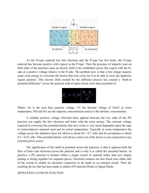
As the N-type material has lost electrons and the P-type has lost holes, the N-type<br />
material has become positive with respect to the P-type. Then the presence of impurity ions on<br />
both sides of the junction cause an electric field to be established across this region with the N-<br />
side at a positive voltage relative to the P-side. The problem now is that a free charge requires<br />
some extra energy to overcome the barrier that now exists for it to be able to cross the depletion<br />
region junction. This electric field created by the diffusion process has created a "built-in<br />
potential difference" across the junction with an open-circuit (zero bias) potential of:<br />
Where: Eo is the zero bias junction voltage, VT the thermal voltage of 26mV at room<br />
temperature, ND and NA are the impurity concentrations and ni is the intrinsic concentration.<br />
A suitable positive voltage (forward bias) applied between the two ends of the PN<br />
junction can supply the free electrons and holes with the extra energy. The external voltage<br />
required to overcome this potential barrier that now exists is very much dependent upon the type<br />
of semiconductor material used and its actual temperature. Typically at room temperature the<br />
voltage across the depletion layer for silicon is about 0.6 - 0.7 volts and for germanium is about<br />
0.3 - 0.35 volts. This potential barrier will always exist even if the device is not connected to any<br />
external power source.<br />
The significance of this built-in potential across the junction, is that it opposes both the<br />
flow of holes and electrons across the junction and is why it is called the potential barrier. In<br />
practice, a PN junction is formed within a single crystal of material rather than just simply<br />
joining or fusing together two separate pieces. Electrical contacts are also fused onto either side<br />
of the crystal to enable an electrical connection to be made to an external circuit. Then the<br />
resulting device that has been made is called a PN junction Diode or Signal Diode.<br />
DEPLETION LAYER PN JUNCTION