

tidu271

Create successful ePaper yourself
Turn your PDF publications into a flip-book with our unique Google optimized e-Paper software.
Power Supply Design and Isolation<br />
www.ti.com<br />
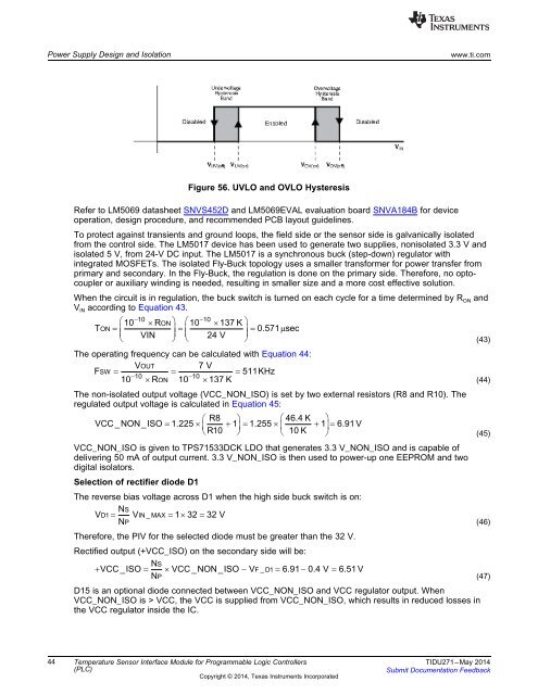
Figure 56. UVLO and OVLO Hysteresis<br />
Refer to LM5069 datasheet SNVS452D and LM5069EVAL evaluation board SNVA184B for device<br />
operation, design procedure, and recommended PCB layout guidelines.<br />
To protect against transients and ground loops, the field side or the sensor side is galvanically isolated<br />
from the control side. The LM5017 device has been used to generate two supplies, nonisolated 3.3 V and<br />
isolated 5 V, from 24-V DC input. The LM5017 is a synchronous buck (step-down) regulator with<br />
integrated MOSFETs. The isolated Fly-Buck topology uses a smaller transformer for power transfer from<br />
primary and secondary. In the Fly-Buck, the regulation is done on the primary side. Therefore, no optocoupler<br />
or auxiliary winding is needed, resulting in smaller size and a more cost effective solution.<br />
When the circuit is in regulation, the buck switch is turned on each cycle for a time determined by R ON and<br />
V IN according to Equation 43.<br />
T<br />
ON<br />
10 10<br />
10 RON<br />
10 137 K <br />
0.571sec<br />
VIN 24 V <br />
<br />
The operating frequency can be calculated with Equation 44:<br />
VOUT<br />
7 V<br />
FSW<br />
511KHz<br />
10 10<br />
10 R ON 10 137 K<br />
<br />
The non-isolated output voltage (VCC_NON_ISO) is set by two external resistors (R8 and R10). The<br />
regulated output voltage is calculated in Equation 45:<br />
R8 46.4 K <br />
VCC _NON_ISO 1.225 1 1.255 1 6.91 V<br />
R10<br />
<br />
10 K <br />
VCC_NON_ISO is given to TPS71533DCK LDO that generates 3.3 V_NON_ISO and is capable of<br />
delivering 50 mA of output current. 3.3 V_NON_ISO is then used to power-up one EEPROM and two<br />
digital isolators.<br />
Selection of rectifier diode D1<br />
The reverse bias voltage across D1 when the high side buck switch is on:<br />
NS<br />
VD1<br />
VIN _ MAX 1 32 32 V<br />
NP<br />
Therefore, the PIV for the selected diode must be greater than the 32 V.<br />
Rectified output (+VCC_ISO) on the secondary side will be:<br />
N<br />
<br />
N<br />
VCC _ISO<br />
S<br />
VCC _NON_ISO VF _ D1 6.91 0.4 V 6.51 V<br />
P<br />
D15 is an optional diode connected between VCC_NON_ISO and VCC regulator output. When<br />
VCC_NON_ISO is > VCC, the VCC is supplied from VCC_NON_ISO, which results in reduced losses in<br />
the VCC regulator inside the IC.<br />
(43)<br />
(44)<br />
(45)<br />
(46)<br />
(47)<br />
44 Temperature Sensor Interface Module for Programmable Logic Controllers TIDU271–May 2014<br />
(PLC)<br />
Submit Documentation Feedback<br />
Copyright © 2014, Texas Instruments Incorporated