


Create successful ePaper yourself
Turn your PDF publications into a flip-book with our unique Google optimized e-Paper software.
a <strong>EVAL</strong>-<strong>AD1852EB</strong><br />
OVERVIEW<br />
The <strong>EVAL</strong>-AD1852-EB evaluation board permits testing and<br />
demonstrating the high-performance AD1852 24-bit stereo<br />
DAC. An input signal is required in either optical or coaxial<br />
SPDIF format or, alternatively, directly via a 10-pin header in<br />
I2S, left justified, right justified, or DSP modes. A second 10-pin<br />
header and DB-9 connector allows control of the internal registers<br />
from an external SPI controller.<br />
Power requirements are a clean 9 V to 12 V dc source for the<br />
digital section and a clean ±12 V dc for the analog section. The<br />
positive supplies can be paralleled if desired. On-board regulators<br />
derive separate “clean” 5 V dc supplies for the digital and analog<br />
sections. Audio output is provided from two RCA phono jacks.<br />
AD1852 OVERVIEW<br />
The AD1852 is a complete 16-/20-/24-bit single-chip digital<br />
audio, stereo digital-to-analog converter (DAC). It is comprised<br />
of a multibit sigma-delta modulator with dither, continuous<br />
time analog filters, and differential analog outputs. Other features<br />
include an on-chip stereo attenuator, de-emphasis filter,<br />
selectable interpolator and mute control, programmed through<br />
REV. 0<br />
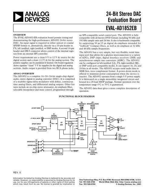
J2 EXT DATA<br />
J1 RCA JACK<br />
SPDIF INPUT<br />
OPTICAL<br />
INPUT<br />
S3<br />
SPDIF/EXT(J2)<br />
S4<br />
DEEMPHASIS<br />
S2<br />
MUTE<br />
S6<br />
RESET<br />
U1<br />
TOS LINK<br />
S1<br />
SIGNAL<br />
SOURCE<br />
SELECT<br />
Information furnished by <strong>Analog</strong> <strong>Devices</strong> is believed to be accurate and<br />
reliable. However, no responsibility is assumed by <strong>Analog</strong> <strong>Devices</strong> for its<br />
use, nor for any infringements of patents or other rights of third parties<br />
which may result from its use. No license is granted by implication or<br />
FUNCTIONAL BLOCK DIAGRAM<br />
U2<br />
DIR<br />
U8<br />
RESET<br />
GENERATOR<br />
U10<br />
U11<br />
RESET<br />
S5<br />
INTERFACE<br />
MODE<br />
U4<br />
I/F<br />
MUX<br />
DS3<br />
DEEMPH<br />
DS4<br />
VERF<br />
JP1<br />
INTERPOLATION<br />
MODE<br />
U5<br />
J3/J5<br />
SPI CONTROL<br />
PORTS<br />
U3<br />
DAC<br />
AD1852<br />
24-Bit Stereo DAC<br />
Evaluation Board<br />
an SPI-compatible serial control port. The AD1852 is fully<br />
compatible with all known DVD formats including 96 kHz and<br />
192 kHz sample rates and 24 bits. It also is backwards-compatible<br />
by supporting 50 µs/15 µs digital de-emphasis intended for<br />
“redbook” Compact Discs, as well as de-emphasis at 32 kHz<br />
and 48 kHz sample frequencies.<br />
The AD1852 has a very simple, but very flexible, serial data<br />
input port that allows for a glueless interconnection to a variety<br />
of ADCs, DSP chips, digital interface receivers (DIR) and<br />
asynchronous sample rate converters (ASRC). The AD1852<br />
can be configured in left-justified (LJ), I2S, right-justified (RJ),<br />
or DSP serial port compatible modes. It can support 16, 20, and<br />
24 bits in all modes. The AD1852 accepts serial audio data in<br />
MSB first, twos complement format. A power-down mode is<br />
offered to minimize power consumption when the device is<br />
inactive. The AD1852 operates from a single 5 V power supply.<br />
It is fabricated on a single monolithic integrated circuit and<br />
housed in a 28-lead SSOP package. Normal operation over the<br />
temperature range 0°C to 70°C is guaranteed.<br />
The AD1852 data sheet gives a more complete description of<br />
operation.<br />
One Technology Way, P.O. Box 9106, Norwood, MA 02062-9106, U.S.A.<br />
Tel: 781/329-4700 World Wide Web Site: http://www.analog.com<br />
Fax: 781/326-8703 © <strong>Analog</strong> <strong>Devices</strong>, Inc., 2001<br />
U9B<br />
U9A<br />
J6<br />
LEFT<br />
J7<br />
RIGHT<br />
DS1<br />
ZERO LEFT<br />
DS2<br />
ZERO RIGHT
<strong>EVAL</strong>-<strong>AD1852EB</strong><br />
FUNCTIONAL DESCRIPTION<br />
The AD1852 evaluation board presents a reference design that<br />
can be used as a suggested layout and circuit implementation,<br />
which will deliver optimal performance from the audio DAC. As<br />
far as is possible on an evaluation board, current assembly methods<br />
and components are used. Most components are surface mount<br />
devices and a four-layer printed circuit board is used with full<br />
internal power and ground planes for best noise performance.<br />
For guidance, a schematic, bill of materials, PLD source code,<br />
and PCB plots are included in this document.<br />
POWER SUPPLIES<br />
The PC board is divided into analog and digital sections, each<br />
with separate power supplies, to facilitate testing. The digital<br />
power supply input is via binding post terminals J8 and J9. The<br />
recommended digital supply is 12 V dc at 110 mA ± 25 mA. An<br />
on-board voltage regulator (U6) provides 5 V dc, ± 5% to the<br />
digital circuitry. The analog power supply inputs are binding<br />
posts, J10, J11, and J12. Recommended analog supply is 12 V<br />
dc at 50 mA ± 10 mA and –12 V dc at –20 ± 5 mA. An onboard,<br />
low noise voltage regulator, (U7) provides 5 V dc, ± 5%<br />
to the analog power pins of the AD1852 DAC.<br />
DIGITAL AUDIO SIGNAL INPUTS<br />
RCA phone jack, (J1) and optical TOSLink input (U1) may be<br />
used for standard SPDIF or AES/EBU input signals. J1 is terminated<br />
with a 75 Ω resistor. Switch S1 selects between J1 and U1<br />
inputs and feeds the selected signal to the digital interface receiver<br />
(U2). Switch SPDIF/EXT (S3) controls CPLD (U4) and U11,<br />
which is used to switch signals between the SPDIF input (J1)<br />
and the direct input, via the 10-pin header J2, EXT DATA<br />
INTERFACE.<br />
The EXT DATA INTERFACE input permits buffered (U4,<br />
M4–64/32 and U11, HC00) access to the BCLK, L/RCLK,<br />
SDATA and MCLK inputs to the AD1852 DAC. This permits<br />
testing with left-justified, I2S or right-justified, serial input modes.<br />
Note that with right-justified input data, the AD1852 control<br />
register must be programmed for the correct number of data<br />
bits, i.e., 16, 20 or 24 bits. When using the direct input header,<br />
it is necessary to provide all four signals, MCLK, BCLK, L/RCLK<br />
and SDATA. A termination network (RC1), consisting of a series<br />
connected 100 Ω resistor and a 47 pF capacitor, is shunted<br />
across each signal line to reduce line reflections. A 10 kΩ pullup<br />
network (RT1) ensures the inputs are not floating in the<br />
absence of an external data source.<br />
EXTERNAL SPI CONTROL PORT<br />
An external control port, SPI CONTROL PORT (J3), is provided,<br />
via a 10-pin header, so that the internal volume controls<br />
and control registers can be programmed from an external host<br />
or microcontroller. This port accepts serial data to independently<br />
set the left/right volume or the operating mode of the<br />
AD1852 by programming the contents of three internal 16-bit<br />
registers. When setting the volume, a 16-bit control word has<br />
14 bits allocated to the left or right volume control, giving a<br />
total range of 84 dB. Details of the signal format and timing are<br />
discussed in the AD1852 data sheet.<br />
–2–<br />
An additional connector, PC PORT (J5), has been provided to<br />
permit connection to the parallel port of a computer. A termination<br />
network (RC2) consisting of a series-connected 100 Ω<br />
resistor and a 47 pF capacitor, is shunted across each signal line<br />
to reduce line reflections. Additionally, a Schmitt trigger (U5)<br />
reduces the effects of noise and line reflections. A 10 kΩ pull-up<br />
network (RT2) ensures the inputs are not floating in the absence<br />
of an external data source.<br />
PC LabView software (LV<strong>AD1852EB</strong>.zip) can be downloaded<br />
from the <strong>Analog</strong> <strong>Devices</strong>, Inc., Digital Audio website, (http://<br />
www.analog.com/techsupt/eb/lin_eb/ad1852/ad1852.html) to<br />
program the internal control registers and set the left and right<br />
volume levels. An interface cable connects between the PC<br />
parallel printer port (LPTn) 25-pin Dsub connector and the<br />
9-pin Dsub (J5) connector on the evaluation board. A suitable<br />
cable is Belkin Modem cable, part number 589604, F2L088-06<br />
The pin-out for this cable in shown, in the table below, for users<br />
who wish to make their own cable.<br />
Table I.<br />
PC <strong>EVAL</strong> Board<br />
Function (DB-25 Male) (DB-9 Female)<br />
Data 6 8 1<br />
Data 1 3 2<br />
Data 0 2 3<br />
GND 20 4<br />
Data 5 7 5<br />
Data 4 6 6<br />
Data 2 4 7<br />
Data 3 5 8<br />
GND 22 9<br />
Chassis Shield GND Case Case<br />
NOTE: When setting the internal control registers via the SPI<br />
port, it is essential to pull the corresponding external pins low as<br />
they are wire-OR’d with the SPI control registers. This applies<br />
to the interpolation mode pins, via JP1 (192/48 P7, 96/48 P10),<br />
the power down/reset pin, (RESET), the mute pin, (MUTE), the<br />
interface mode pins (IDPM1, IDPM0) and the de-emphasis<br />
control pin, (DEEMPH). Also note that when the right-justified<br />
interface mode is selected, either via the external pins or via the<br />
SPI port, the default data word width is 24 bits. It is necessary<br />
to select 16 or 20 bits via the SPI control register if these word<br />
lengths are required.<br />
AUDIO SIGNAL OUTPUTS<br />
RCA jacks J6 and J7 provide LEFT and RIGHT audio output<br />
signals. The output is filtered with a low-pass anti-image filter<br />
using an OP275 audio op amp (U9) which also converts the differential<br />
outputs of the AD1852 to single ended signals. The<br />
filter –3 dB cut-off frequency is 100 kHz and has an approximate<br />
Third Order Bessel (linear phase) response. The output<br />
source impedance is approximately 600 Ω. The full-scale output<br />
signal is 2 V rms (5.6 V p-p).<br />
REV. 0
SWITCH AND JUMPER FUNCTIONS<br />
• S1 is used to select between the RCA SPDIF INPUT (J1) and<br />
the TOSLINK optical input, (U1). The SPDIF signal is a<br />
self-clocking, Manchester-encoded signal that is decoded by<br />
the digital interface receiver (DIR, U2) to extract the left and<br />
right digital audio data and associated status signals.<br />
• S2 is used to activate the AD1852 MUTE hardware function.<br />
• S3 switches the CPLD (U4) digital input signals between the<br />
digital interface receiver (DIR, U2) and the EXT DATA<br />
INTERFACE (J2). The CPLD (U4) digital outputs go directly<br />
to the AD1852 DAC. In addition to the digital audio data<br />
signals, S3 also switches the master clock between the DIR<br />
(U2) and the Ext Data I/F input (J2) via the NAND gate (U11).<br />
• S4 is used to enable the internal AD1852 DEEMPHASIS<br />
digital filter. This is confirmed by lighting the DEEMPH<br />
LED, (DS3).<br />
• S5 selects the serial interface modes for the SPDIF receiver<br />
(U2) and the AD1852 DAC (U3):<br />
REV. 0<br />
Table II. Serial Interface Mode Selection<br />
S5<br />
Position AD1852 Serial Interface Mode IDPM1 IDPM0<br />
0 Left Justified, 16 to 24 Bits 1 0<br />
1 I2S, 16 to 24 Bits 0 1<br />
2 Right Justified, (U2 (DIR) is<br />
set for 24 Bits. Program the<br />
AD1852 via the SPI port for<br />
24 Bits if using U2).<br />
0 0<br />
3 DSP Word Sync, 16- to 24-Bits 1 1<br />
4 Serial Mode is set through SPI<br />
Port using LabView Software.<br />
0 0<br />
5 Spare – Not Used<br />
6 Spare – Not Used<br />
7 Spare – Not Used<br />
• S6 provides a RESET function via reset generator U8<br />
(ADM811TART) and a “clean” 200 ms delay after release.<br />
U8 also provides a 200 ms delayed reset release at power-up.<br />
This ensures that the digital interface receiver (DIR, U2) and<br />
the AD1852 are correctly initialized after power-up and their<br />
internal registers are set to the correct default values.<br />
• JP1 Header is used to select the internal interpolation ratio for<br />
the AD1852. Jumpers are selected according to the following<br />
table. The default is 8× interpolation, i.e., both jumpers are<br />
installed. NOTE: When the internal registers are used, the<br />
effective logic state is the logical OR of the external pin and<br />
the program register, hence both jumpers should be in place<br />
so that the programmable registers can correctly set the state<br />
of the control bits.<br />
Table III.<br />
Interpolation Ratio (SR) 96/48 (JP1-1) 192/48 (JP1-2)<br />
8× (32 kHz to 50 kHz) 0 0<br />
4× (64 kHz to 100 kHz) 0 1<br />
2× (128 kHz to 200 kHz) 1 0<br />
Not Allowed 1 1<br />
Note: 0 = Closed.<br />
–3–<br />
<strong>EVAL</strong>-<strong>AD1852EB</strong><br />
Indicator Display LEDs<br />
Five red LED indicators are provided for status indication.<br />
• Display LEDs DS1, ZL and DS2, ZR show that the AD1852<br />
is detecting a zero signal in either the left or right channel<br />
respectively.<br />
• Display LED DS3, DEEMPH, indicates that either switch S4<br />
has selected de-emphasis or that the incoming SPDIF signal<br />
has the EMPHASIS status bit set. In either case, illumination<br />
of DS3 indicates that the DEEMPHASIS filter function of the<br />
AD1852 is active.<br />
• Display LED DS4, VERF, indicates that the digital interface<br />
receiver has detected an error condition in the received SPDIF<br />
signal or the SPDIF Invalid status bit has been set.<br />
• Display LED DS5, POWER, shows the presence of 5 V dc on<br />
the analog 5 V power supply.<br />
INTEGRATED CIRCUIT FUNCTIONS<br />
There are 11 active devices on the AD1852 evaluation board.<br />
Following is a brief description of the function of each part.<br />
• U1 (TORX173) is the Toshiba Digital Audio Optical<br />
(TOSLink) Receiver. This part accepts a visible red SPDIFmodulated<br />
signal and converts it to a standard TTL digital<br />
signal suitable for input to the digital audio receiver (U2).<br />
• U2 (CS8414-CS) digital audio interface receiver, (DIR) receives<br />
and decodes the serial SPDIF, digital audio encoded signal.<br />
This signal is Manchester modulated and is self-clocked at a<br />
multiple of the encoded SPDIF sample rate. Four digital<br />
audio signals are decoded by the CS8414. The serial data<br />
SDATA, the master clock at 256 FS, MCLK, the left/right<br />
frame clock L/RCLK and the serial bit clock at 64 FS, BCLK.<br />
• U3 (AD1852JRS) is the high performance stereo DAC.<br />
Depending upon selected modes of operation, (JP1) sample<br />
rates up to 192 kHz and 24 bits may be tested by changing the<br />
internal interpolation ratio. The interface mode can be selected<br />
for Left Justified (LJ), I2S or Right Justified (RJ) by means of<br />
the Interface Mode switch (S5). Internal registers of the<br />
AD1852 can be programmed via the PC Port (J5) or via the<br />
SPI Control Port, header (J3). Mute is controlled directly by<br />
the control switch S2. The De-emphasis filter can be turned<br />
on with the switch DEEMPH (S4) or pre-emphasis may be<br />
detected and enabled by the SPDIF receiver.<br />
• U4 (M4-64/32) is a Vantis CPLD and has been programmed<br />
to provides input signal MUX selection, LED buffering and<br />
switch decoding for the different interface modes. The output<br />
interface mode of the DIR (U2) must be compatible with the<br />
input to the AD1852 (U3) and this is selected at the same<br />
time as the mode for the AD1852 is selected, with switch<br />
Interface Mode (S5). S5 is decoded to drive the DIR mode<br />
pins (M0-3) and AD1852 mode pins (IDPM0) and (IDMP1).<br />
The source code in included in Appendix A. Note: Because of<br />
excessive jitter degradation in CPLDs, a separate IC (U11) is<br />
used to select the MCLK input to the AD1852.<br />
• U5 (74HC14) provides Schmitt trigger buffering for the SPI<br />
Control Port (J3) and PC Port (J5) signals. This helps to<br />
reduce problems due to noise and ringing on the signal lines.<br />
• U6 (LM317) provides 5 V dc low voltage regulation for the<br />
digital section of the evaluation board.
<strong>EVAL</strong>-<strong>AD1852EB</strong><br />
• U8 (ADM811TART) is a RESET generator that provides<br />
a debounced 200 ms reset signal from the push button (S3)<br />
or on power up. The reset is active if the 5 V supply drops<br />
below 3 V.<br />
• U7 (AD3303-5.0) is a low noise 5 V dc regulator for the analog<br />
section of the AD1852.<br />
• U9 (OP275) is a low noise and distortion, audio op amp. U9<br />
provides differential-to-single-ended conversion and a lowpass<br />
anti-image filter. A third order low-pass Bessel filter<br />
response is implemented with a –3 dB corner frequency of<br />
100 kHz and a 60 dB/decade roll-off. This type of filter is<br />
characterized by a linear phase response and fast transient<br />
response without overshoot.<br />
• U10 (74HC00) is used to provide a reset code to the digital<br />
interface receiver (U2), pins M0–3, at power up and also sends<br />
the correct interface code to ensure the digital output format<br />
matches the input of the DAC.<br />
• U11 (74HC00) is used to select the correct master clock<br />
source for the DAC when it is switched between the SPDIF<br />
receiver (U2) and the Ext Data Interface (J2). A discrete logic<br />
gate is used for this function, because of the excessive jitter<br />
that modulates high-frequency clock signals when they are<br />
handled by PLDs.<br />
–4–<br />
PERFORMANCE SPECIFICATIONS<br />
Typical performance, for a sample rate of 48 kHz, is tabulated<br />
below.<br />
1. SNR, A-Weighted –114 dBFS ± 1 dB<br />
2. DNR, A-Weighted –114 dBFS ± 1 dB<br />
3. THD+N –102 dBFS ± 2 dB<br />
4. Frequency Response ± 0.2 dB, 10 Hz to 20 kHz<br />
5. Noise Floor –145 dBFS<br />
6. Full-Scale Audio Output 2 V rms<br />
ATTACHMENTS<br />
The following is included for your convenience.<br />
• Appendix A: ABEL Source Code for Vantis MACH4-64/32<br />
CPLD.<br />
• Appendix B: Set of Schematics, Figures 1 and 2.<br />
• Appendix C: PCB plots showing the silkscreen layer, top<br />
signal layer, ground planes, power planes, and the bottom<br />
signal layer, Figures 3–7.<br />
FURTHER INFORMATION<br />
Ordering information: order number is <strong>EVAL</strong>-<strong>AD1852EB</strong>.<br />
For application questions, please contact our Central Applications<br />
Department at 1-781-937-1428 for assistance.<br />
REV. 0
REV. 0<br />
APPENDIX A<br />
–5–<br />
<strong>EVAL</strong>-<strong>AD1852EB</strong><br />
MODULE IF_Logic<br />
TITLE ‘AD1852 EVB Logic’<br />
//===================================================================================<br />
// FILE: 1852ext.abl<br />
// REVISION DATE: 11-01-99 (comment revisions on 2-9-00)<br />
// REVISION BY: Brian Wachob<br />
// REVISION: 3.0 (plus comments)<br />
//<br />
//<br />
// PREVIOUS FILE: 1852r9.abl, AD1852v8.abl<br />
// PREVIOUS DATE: 10-01-99<br />
// PREVIOUS REVISION: 2.0<br />
//<br />
// ORIGINAL AUTHOR: Larry Hurst<br />
//<br />
// BOARD REV.: This code is written for the “AD185_ REV 1” eval. boards<br />
// (with, of course, an AD1852 DAC installed on the eval. board)<br />
//<br />
// DESCRIPTION:<br />
//<br />
// This chip selects between the External Data Interface header (J2) and the<br />
// onboard CS8414 DIR (U2) for the AD1852 DAC input signals, depending upon<br />
// the SPDIF/EXT switch position (S3). When the DIR is the selected signal<br />
// source the digital audio signals, SDATA, BCLK and LRCLK also appear at the<br />
// external Data Interface header (J2) as outputs.<br />
//<br />
// It also decodes the Interface Mode Switch(S5) and sets the interface mode<br />
// pins for both the CS8414 DIR and the AD1852 DAC and corrects the CS8414<br />
// output signals for LJ, RJ, and DSP modes, to match the signal requirements<br />
// for the AD1852.<br />
//<br />
// It also decodes signals from LabView SPI port control software so that it<br />
// can correctly set the interface mode pins for the CS8414 and correctly<br />
// format the CS8414 output signal for LJ, RJ, and DSP modes. (This<br />
// functionality is required when the SPI port is used to set the data format<br />
// used by the DAC instead of setting it directly via the IDPM pins with the<br />
// Interface Mode Switch, S5.)<br />
//<br />
// It also decodes the Deemphasis control signal from the CS8414 (U2) and<br />
// DEEMPH switch(S4), enables and buffers the output master clock and the<br />
// VERF signal from the CS8414.<br />
//<br />
// Finally, the CPLD buffers and drives the status LEDs.<br />
//<br />
//=============================================================================<br />
LIBRARY ‘MACH’;<br />
MACH_SLEW(FAST,2,MCLK:MCLKO);<br />
DECLARATIONS<br />
// IF_Logic DEVICE ‘M4-64/32-15VC’;<br />
“INPUTS ———————————————————————————————————<br />
// TDI, TCK, TMS pin 4, 7, 26; //JTAG I/P’s<br />
SLCT_C, SLCT_B, SLCT_A pin 15, 19, 14; //Interface Mode Select<br />
ISDATA, IMCLK, ILRCLK, IBCLK pin 1, 5, 9, 10; //DIR I/P’s<br />
VERF, NPREEMPH, NDEEMPH pin 44, 8, 13; //DAC Control<br />
SPDIF_EXT pin 12; //DAC Signal Source Select<br />
ZR, ZL pin 24, 34; //DAC ZERO Signals<br />
EMCLK pin 27; //External MCLK Input
<strong>EVAL</strong>-<strong>AD1852EB</strong><br />
MODCLK pin 40; /<br />
/Clocks in serial mode codes<br />
MODSTM pin 37; /<br />
/Serial mode code stream from CPU<br />
“OUTPUTS ———————————————————————————————————<br />
// TDO pin 29; //JTAG O/P<br />
M0, M1, M2 pin 3, 2, 18 istype ‘com’; //DIR Mode Select<br />
IDPM0, IDPM1 pin 35, 36 istype ‘com’; //DAC Mode Select<br />
MCLK, BCLK, LRCLK pin 30, 32, 33 istype ‘com’; //DAC Digital Data<br />
SDATA pin 31 istype ‘com’;<br />
MCLKO pin 23 istype ‘com’; //Ext MCLK Drive<br />
DEEMPH pin 25 istype ‘com’; //DAC Deemphasis Control<br />
NLVERF, NLZL, NLZR, NLDEEMPH pin 11, 21, 22, 20 istype ‘com’; //LED Status Drive<br />
ESDATA, ELRCLK, EBCLK pin 43, 42, 41 istype ‘com’; //External Data I/Os<br />
// Registers for delaying the data in RJ and DSP modes<br />
// such that it is output in the correct format<br />
// to match the signal requirements for the AD1852.<br />
“NODES<br />
QA, QB, QC, QD, QE, QF node istype ‘reg, buffer’;<br />
QG, QH, QI, QJ, QK, QL node istype ‘reg, buffer’;<br />
Q20, Q24 node istype ‘reg, buffer’;<br />
QDSP node istype ‘reg, buffer’;<br />
// Shift register for reading/holding mode codes<br />
// streaming in from CPU’s LabView control program.<br />
QM0, QM1, QM2, QM3 node istype ‘reg, buffer’;<br />
“MACROS // S5 position 4, External Mode Control<br />
XMODC = (!SLCT_C & SLCT_B & SLCT_A);<br />
//EQUATIONS<br />
// S5 position 0, LabView selection 1, LJ, Invert DIR BCLK<br />
LJ = ( SLCT_C & SLCT_B & SLCT_A)<br />
# ( XMODC & ( (!QM3 & QM2 & !QM1 & QM0)<br />
# ( QM3 & !QM2 & QM1 & !QM0) ) );<br />
// S5 position 1, LabView selection 2, I2S<br />
I2S = ( SLCT_C & SLCT_B & !SLCT_A)<br />
# ( XMODC & ( (!QM3 & QM2 & QM1 & QM0)<br />
# ( QM3 & QM2 & QM1 & !QM0)<br />
# ( QM3 & QM2 & !QM1 & QM0)<br />
# ( QM3 & !QM2 & QM1 & QM0) ) );<br />
// S5 position 2, LabView selection 4, RJ_24, 24-Bit<br />
RJ_24 = ( SLCT_C & !SLCT_B & SLCT_A)<br />
# ( XMODC & ( (!QM3 & !QM2 & !QM1 & QM0)<br />
# (!QM3 & !QM2 & QM1 & !QM0)<br />
# (!QM3 & QM2 & !QM1 & !QM0)<br />
# ( QM3 & !QM2 & !QM1 & !QM0) ) );<br />
// S5 position 3, LabView selection 3, DSP WSync, Delay SDATA<br />
DSP = ( SLCT_C & !SLCT_B & !SLCT_A)<br />
# ( XMODC & (!QM3 & !QM2 & !QM1 & !QM0) );<br />
// LabView selection 5, RJ_20, 20-Bit<br />
RJ_20 = ( XMODC & ( (!QM3 & !QM2 & QM1 & QM0)<br />
# (!QM3 & QM2 & QM1 & !QM0)<br />
# ( QM3 & QM2 & !QM1 & !QM0)<br />
# ( QM3 & !QM2 & !QM1 & QM0) ) );<br />
–6–<br />
REV. 0
LabView selection 6, RJ_16, 16-Bit<br />
RJ_16 = ( XMODC & ( QM3 & QM2 & QM1 & QM0) );<br />
“=============================================================================<br />
EQUATIONS<br />
// Registers holding streaming mode codes from CPU’s LabView control program.<br />
[QM3, QM2, QM1, QM0] := [QM2, QM1, QM0, MODSTM];<br />
[QM3, QM2, QM1, QM0].clk = MODCLK;<br />
// AD1852 DAC Interface Mode Select<br />
IDPM0 = !XMODC & (I2S # DSP);<br />
IDPM1 = !XMODC & (LJ # DSP);<br />
// CS8414 DIR Interface Mode Select<br />
M0 = !RJ_16;<br />
M1 = !I2S;<br />
M2 = !(DSP # RJ_16);<br />
// External I/O Data Port Output Enabled by SPDIF_EXT<br />
ESDATA.oe = SPDIF_EXT;<br />
ELRCLK.oe = SPDIF_EXT;<br />
EBCLK.oe = SPDIF_EXT;<br />
REV. 0<br />
ESDATA = SPDIF_EXT & SDATA;<br />
ELRCLK = SPDIF_EXT & LRCLK;<br />
EBCLK = SPDIF_EXT & BCLK;<br />
// Shift register for DSP, RJ_20, and RJ_24 modes<br />
[QL, QK, QJ, QI, QH, QG, QF, QE, QD, QC, QB, QA] := [QK, QJ, QI,<br />
QH, QG, QF, QE, QD, QC, QB, QA, ISDATA];<br />
[Q24, Q20] := [QH, QL];<br />
QDSP := QA;<br />
[QL, QK, QJ, QI, QH, QG, QF, QE, QD, QC, QB, QA].clk = !IBCLK;<br />
[Q24, Q20].clk = IBCLK;<br />
QDSP.clk = IBCLK;<br />
// AD1852 DAC DAU Signals<br />
SDATA = SPDIF_EXT &(ISDATA &(LJ # I2S # RJ_16)<br />
# DSP & QDSP # RJ_20 & Q20 # RJ_24 & Q24) # !SPDIF_EXT & ESDATA;<br />
LRCLK = SPDIF_EXT & ILRCLK # !SPDIF_EXT & ELRCLK;<br />
BCLK = SPDIF_EXT & ((LJ # RJ_20 # RJ_24) & !IBCLK<br />
# (I2S # DSP # RJ_16) & IBCLK) # !SPDIF_EXT & EBCLK;<br />
MCLK = SPDIF_EXT & IMCLK<br />
# !SPDIF_EXT & EMCLK;<br />
// DAC Deemphasis Control Signal<br />
DEEMPH = !NPREEMPH # !NDEEMPH;<br />
// Slave MCLK for SPI output port<br />
MCLKO = !MCLK;<br />
// LED Status Driver Outputs - LED lights when output low<br />
NLVERF = !VERF;<br />
NLZL = !ZL;<br />
NLZR = !ZR;<br />
NLDEEMPH = !DEEMPH;<br />
“==============================================================================<br />
END IF_Logic<br />
–7–<br />
<strong>EVAL</strong>-<strong>AD1852EB</strong>
<strong>EVAL</strong>-<strong>AD1852EB</strong><br />
JP1 – AD1852 MCLK/SR SELECT<br />
R5<br />
10k<br />
DVDD<br />
DVDD<br />
RC1<br />
RCNTWK<br />
MCLK<br />
xFs<br />
256,384,512,768,1024<br />
128,192,256,384,512<br />
64,96,128,192,256<br />
INTERNAL<br />
CLKRATE<br />
INTERP<br />
RATIO<br />
MODE<br />
96/48 192/48<br />
SAMPLE<br />
RATE<br />
DVDD<br />
J4<br />
ISP PORT<br />
1<br />
DVDD<br />
128Fs<br />
64Fs<br />
32Fs<br />
PROHIBITED MODE<br />
8x<br />
4x<br />
2x<br />
0<br />
0<br />
1<br />
1<br />
0<br />
1<br />
0<br />
1<br />
32-48<br />
96<br />
192<br />
R4<br />
10k<br />
R37<br />
10k<br />
JP1<br />
SELECT<br />
TCK<br />
TMS<br />
TDI<br />
TDO<br />
11<br />
12<br />
U11D<br />
3 13 HC00<br />
MODE<br />
IDPM0<br />
AD1852 INTERFACE<br />
I/F MODE IDPM1<br />
LJ, 16-/20-/24-BIT 1<br />
I2S, 16-/20-/24-BIT 0<br />
RJ 24-BIT (DEFAULT) 0<br />
DSP MODE<br />
1<br />
SPI CONTROL 0<br />
S5<br />
POSN<br />
0<br />
1<br />
2<br />
3<br />
4<br />
8 MCLK<br />
U11C<br />
HC00<br />
9<br />
10<br />
U11A<br />
HC00<br />
1<br />
2<br />
1 1<br />
2 ESDATA 10<br />
R1 C1<br />
3 ELRCLK 9<br />
R2<br />
R2 C2<br />
4<br />
8<br />
R4<br />
EBCLK<br />
R3 C3<br />
5<br />
R6<br />
7<br />
R4 C4<br />
R8<br />
6<br />
6<br />
DVDD<br />
1<br />
J2<br />
C43<br />
100nF<br />
2<br />
3<br />
4<br />
5<br />
R1<br />
R3<br />
R5<br />
R7<br />
GND GND<br />
GND GND<br />
10<br />
9<br />
8<br />
7<br />
U11B<br />
HC00<br />
4<br />
5<br />
EXT DATA INTERFACE<br />
6<br />
0<br />
1<br />
0<br />
1<br />
0<br />
EMCLK<br />
DVDD<br />
DVDD<br />
DVDD<br />
AVDD<br />
C11<br />
100nF<br />
C10<br />
100nF<br />
DVDD<br />
R35<br />
10k<br />
C6<br />
100nF<br />
FB5<br />
600Z<br />
28 18<br />
DVDD AVDD<br />
C7<br />
100nF<br />
D4<br />
DVDD FB4<br />
600Z<br />
C20<br />
C21<br />
100nF FB2 100nF<br />
600Z<br />
TO PIN 21 TO PIN 8<br />
22 7<br />
VA VD<br />
10k<br />
R7<br />
AD1852<br />
STEREO DAC<br />
17<br />
96/48<br />
192/48<br />
NC<br />
SDATA<br />
L/RCLK<br />
BCLK<br />
MCLK<br />
10<br />
7<br />
6<br />
27<br />
25<br />
26<br />
2<br />
IDPM1<br />
IDPM0<br />
ZL<br />
L/RCLK<br />
BCLK<br />
SDATA<br />
LOUT<br />
OUTL<br />
APPENDIX B – Schematics<br />
LOUT<br />
16<br />
SDATA<br />
L/RCLK<br />
BCLK<br />
MCLK<br />
OUTL<br />
U3<br />
AD1852JRS<br />
OUTR<br />
IDPM0<br />
IDPM1<br />
21<br />
20<br />
IDPM0<br />
IDPM1<br />
ROUT<br />
12<br />
DEEMPH<br />
9<br />
DEEMPH<br />
ROUT<br />
13<br />
OUTR<br />
MUTE<br />
DEEMPH<br />
ZR<br />
MCLKO<br />
LZR<br />
LZL<br />
LDEEMPH<br />
SLCT_B<br />
M2<br />
SLCT_C<br />
SLCT_A<br />
DEEMPH<br />
37<br />
36<br />
35<br />
34<br />
33<br />
32<br />
31<br />
30<br />
25<br />
24<br />
23<br />
22<br />
21<br />
20<br />
19<br />
18<br />
15<br />
14<br />
13<br />
I/O31<br />
I/O30<br />
I/O29<br />
I/O28<br />
I/O27<br />
I/O26<br />
I/O25<br />
I/O24<br />
I/O23<br />
I/O22<br />
I/O21<br />
I/O20<br />
I/O19<br />
I/O18<br />
I/O17<br />
I/O16<br />
I/O15<br />
I/O14<br />
I/O13<br />
16 38<br />
TDI VCC VCC TCK<br />
TMS<br />
TDO<br />
CLK0/10<br />
CLK1/11<br />
I/O0<br />
I/O1 U4<br />
I/O2 M4-64/32<br />
I/O3<br />
I/O4 INTERFACE<br />
I/O5 CPLD<br />
I/O6<br />
I/O7<br />
I/O8<br />
I/O9<br />
I/O10<br />
I/O11<br />
I/O12<br />
6 17 28 39<br />
GND<br />
–8–<br />
GND<br />
GND<br />
GND<br />
TDI 4<br />
TCK 7<br />
TMS26<br />
TDO29<br />
IMCLK 5<br />
EMCLK 27<br />
D3 40<br />
EBCLK 41<br />
ELRCLK 42<br />
ESDATA 43<br />
VERF 44<br />
ISDATA 1<br />
M1 2<br />
M0 3<br />
PREEMPH 8<br />
ILRCLK 9<br />
IBCLK 10<br />
LVERF 11<br />
SPDIF/EXT 12<br />
SPIDIF/EXT<br />
26 ISDATA<br />
11 ILRCLK<br />
12 IBCLK<br />
19 IMCLK<br />
S3<br />
SPDIF/EXT<br />
SDATA<br />
FSYNC<br />
SCK<br />
MCK<br />
SPDIF RCVR<br />
23 M0<br />
24 M1<br />
18 M2<br />
17 M3<br />
M0<br />
M1<br />
M2<br />
M3<br />
U2<br />
CS8414–CS<br />
C1<br />
10nF<br />
J1<br />
1<br />
SPDIF I/P SIGNAL SOURCE<br />
0<br />
S1<br />
75.0<br />
R1<br />
1<br />
14<br />
15<br />
28<br />
25<br />
C<br />
U<br />
CBL<br />
VERF<br />
ERF<br />
9<br />
RXP<br />
10<br />
RXN<br />
C2<br />
10nF<br />
23<br />
3<br />
4<br />
5<br />
8<br />
22<br />
DVDD<br />
MUTE<br />
C22<br />
15 F 10V TANT<br />
14<br />
C9<br />
100nF<br />
FILTR<br />
CLATCH<br />
CCLK<br />
CDATA<br />
C5<br />
100nF<br />
19<br />
FILTB<br />
ZEROR<br />
ZEROL<br />
CLAT<br />
CCLK<br />
CDATA<br />
ZR<br />
ZL<br />
DVDD<br />
6<br />
5<br />
4<br />
3<br />
2<br />
27<br />
16<br />
13<br />
C0/E0<br />
Ca/E1<br />
Cb/E2<br />
Cc/F0<br />
Cd/F1<br />
Ce/F2<br />
SEL<br />
CS12/FCK<br />
FB1<br />
600Z<br />
C4<br />
100nF<br />
20 FILT<br />
3<br />
R3<br />
475<br />
1<br />
OUT<br />
DVDD<br />
TOSLINK I/P<br />
15<br />
AGND<br />
AGND<br />
DGND<br />
RESET<br />
11<br />
24<br />
RST<br />
C23<br />
15 F 10V TANT<br />
DGND<br />
8<br />
AGND<br />
21<br />
C19<br />
68nF<br />
DGND<br />
DGND<br />
SHLD<br />
SHLD<br />
AGND<br />
DGND<br />
2<br />
4<br />
5<br />
6<br />
U1<br />
TORX173<br />
FB3<br />
600Z<br />
DVDD<br />
C8<br />
100nF<br />
12 CLAT<br />
HC14<br />
U5F<br />
13<br />
HC14<br />
2<br />
U5A<br />
1<br />
DVDD<br />
DVDD<br />
U5B<br />
3<br />
DS4<br />
392<br />
10 CCLK<br />
HC14<br />
U5E<br />
11<br />
HC14<br />
4<br />
VERF<br />
R15<br />
LVERF<br />
DS3<br />
392<br />
DEEMPHASIS<br />
R14<br />
LDEEMPH<br />
8 CDATA<br />
HC14<br />
U5D<br />
9<br />
HC14<br />
6<br />
U5C<br />
5<br />
DS2<br />
392<br />
ZERO RIGHT<br />
R12<br />
LZR<br />
DVDD<br />
DS1<br />
392<br />
ZERO LEFT<br />
R13<br />
LZL<br />
RT2<br />
10k NTWK<br />
2<br />
3<br />
4<br />
5<br />
R1<br />
R3<br />
R5<br />
R7<br />
GND GND<br />
R2<br />
R4<br />
R6<br />
10<br />
9<br />
8<br />
7<br />
2<br />
3<br />
4<br />
5<br />
C1<br />
C2<br />
C3<br />
C4<br />
GND GND<br />
R1<br />
R2<br />
R3<br />
R4<br />
RC2<br />
RCNTWK<br />
10<br />
9<br />
CLAT 8<br />
7<br />
DVDD<br />
C41<br />
C42 100nF<br />
100nF<br />
J3<br />
SPI CONTROL PORT<br />
DVDD<br />
1<br />
CDATA<br />
CCLK<br />
3 M0<br />
U10A<br />
HC00<br />
1<br />
2<br />
DEEMPH<br />
M0<br />
MUTE<br />
6 M1<br />
8 M2<br />
4<br />
U10B<br />
5 HC00<br />
9<br />
U10C<br />
10 HC00<br />
DVDD<br />
M1<br />
R10<br />
10k<br />
10k<br />
R8<br />
Figure 1. SPDIF Receiver, Interface CPLD and AD1852 DAC Circuits<br />
R2<br />
3.40k<br />
1<br />
1<br />
1<br />
M2<br />
R11<br />
10k<br />
11 M3<br />
12<br />
U10D<br />
13 HC00<br />
RST<br />
DVDD<br />
DVDD<br />
R8<br />
SLCT_A<br />
SLCT_B<br />
SLCT_C<br />
R9<br />
S5<br />
10k<br />
INTERFACE MODE<br />
1<br />
2 2<br />
4<br />
C<br />
S4<br />
DEEMPH<br />
4<br />
0<br />
DVDD<br />
6<br />
6<br />
MCLKO<br />
D0<br />
D2<br />
D1<br />
R36<br />
10k<br />
S5<br />
MODE<br />
6<br />
10k<br />
R6<br />
5<br />
9<br />
4<br />
8<br />
3<br />
7<br />
2<br />
6<br />
1<br />
D3<br />
D4<br />
S2<br />
MUTE<br />
J5<br />
PCPORT<br />
CS8414 OUTPUT<br />
I/F MODE FORMAT<br />
LEFT – JUST INV SCK, 16-/24-BIT<br />
12S, 16-/24-BIT, 1 LSB DELAY<br />
RIGHT JUST, 24-BIT<br />
DSP WSYNC, 16-/24-BIT<br />
SPI CONTROLLED<br />
0<br />
1<br />
2<br />
3<br />
4<br />
5<br />
6<br />
REV. 0
9-12<br />
VOLTS<br />
DGND<br />
+12V<br />
J8<br />
REV. 0<br />
CR3<br />
DL4001<br />
CR1<br />
1SMB15AT3<br />
J9<br />
J10<br />
CR2<br />
SMB15AT3<br />
AGND<br />
–12V<br />
J11<br />
J12<br />
CR4<br />
DL4001<br />
FB7<br />
600Z<br />
FB6<br />
600Z<br />
C14<br />
100nF<br />
C37<br />
47 F 16V A1<br />
C35<br />
47 F 16V A1<br />
RESET GENERATOR<br />
3<br />
RESET S6<br />
3<br />
U6<br />
LM317MDT<br />
VIN VOUT 4<br />
C12<br />
100nF<br />
C16<br />
100nF<br />
GND<br />
1<br />
C24<br />
15 F 10V TANT<br />
U7<br />
ADP3303–5.0<br />
8<br />
IN OUT<br />
1<br />
7<br />
IN OUT<br />
2<br />
6<br />
ERR NR<br />
3<br />
5<br />
SD GND<br />
4<br />
DVDD<br />
U8<br />
4 ADM811TART<br />
VCC<br />
MR RESET<br />
GND<br />
1<br />
DGND<br />
5V REG<br />
C3<br />
10nF<br />
R33<br />
243<br />
R34<br />
715<br />
C15<br />
100nF<br />
2 RST<br />
5V REG<br />
DVDD<br />
C13 C36<br />
100nF 47 F 16V A1<br />
LOUT<br />
C39<br />
47 F 16V A1<br />
C38<br />
47 F<br />
16V A1<br />
AGND<br />
DGND<br />
R16<br />
392<br />
C40<br />
47 F 16V A1<br />
DS5<br />
POWER<br />
–9–<br />
AV CC<br />
AVDD<br />
ROUT<br />
AV CC<br />
LOUT<br />
ROUT<br />
R39<br />
OPTION<br />
R38<br />
OPTION<br />
R21<br />
2.80k<br />
C30<br />
1.0nF NP0<br />
C29<br />
2.7nF PPS<br />
R23<br />
806<br />
R24<br />
1.0k<br />
R22<br />
3.01k<br />
R17<br />
1.50k<br />
R18<br />
499<br />
AGND<br />
PLEASE NOTE: R38, R39<br />
OPTIONAL RESISTORS.<br />
TRIM TO REDUCE THD<br />
WITH AD1855 UP TO 6dB<br />
R25<br />
2.80k<br />
C32<br />
1.0nF NP0<br />
C31<br />
2.7nF PPS<br />
R27<br />
806<br />
R28<br />
1.0k<br />
R26<br />
3.01k<br />
R19<br />
1.50k<br />
R20<br />
499<br />
AGND<br />
2<br />
3<br />
<strong>EVAL</strong>-<strong>AD1852EB</strong><br />
C25<br />
270pF NP0<br />
U9B<br />
6<br />
5<br />
OP275GP<br />
7<br />
R29<br />
549<br />
C33<br />
2.2nF PPS<br />
C26<br />
AVCC 820pF NP0<br />
C17<br />
100nF<br />
C27<br />
270pF NP0<br />
U9A<br />
OP275GP<br />
C28<br />
820pF NP0<br />
1<br />
C18<br />
100nF<br />
AV CC<br />
C34<br />
2.2nF PPS<br />
Figure 2. Anti-Image Filters, Power Supply Regulation, Reset Generator<br />
J6<br />
1<br />
LEFT OUT<br />
0<br />
R31<br />
53.6k<br />
BESSEL LP FILTER RESPONSE<br />
CORNER FREQUENCY: 100kHz<br />
–0.11dB @ 20kHz<br />
–0.45dB @ 40kHz<br />
STEP RESPONSE:<br />
<strong>EVAL</strong>-<strong>AD1852EB</strong><br />
APPENDIX C – Printed Circuit Board<br />
Figure 3. Silk Screen<br />
Figure 4. Top Layer (Component Side)<br />
–10–<br />
REV. 0
REV. 0<br />
Figure 5. Ground Planes<br />
Figure 6. Power Planes<br />
–11–<br />
<strong>EVAL</strong>-<strong>AD1852EB</strong>
<strong>EVAL</strong>-<strong>AD1852EB</strong><br />
Figure 7. Bottom Layer (Solder Side)<br />
–12–<br />
REV. 0
REV. 0<br />
APPENDIX D – Parts List<br />
Bill of Materials for <strong>AD1852EB</strong><br />
–13–<br />
<strong>EVAL</strong>-<strong>AD1852EB</strong><br />
Qty.<br />
Used Part Type Designator Footprint Description<br />
3 10nF C1, C2, C3 SMD 0805 10%, 50 V, X7R Multilayer Ceramic Capacitor<br />
20 100nF C4, C5, C6, C7, C8, C9,<br />
C10, C11, C12, C13, C14,<br />
C15, C16, C17, C18,<br />
C20, C21, C41, C42, C43<br />
SMD 0805 10%, 50 V, X7R Multilayer Ceramic Capacitor<br />
1 68nF C19 SMD 0805 10%, 50 V, X7R Multilayer Ceramic Capacitor<br />
3 15uF 10V Tant C22, C23, C24 EIA Size B 20%, 10 VW, Tantalum Electrolytic Capacitor<br />
2 270pF NP0 C25, C27 SMD 0805 5%, 50 V, NP0 Multilayer Ceramic Chip Capacitor<br />
2 820pF NP0 C26, C28 SMD 0805 5%, 50 V, NP0 Multilayer Ceramic Chip Capacitor<br />
2 2.7nF PPS C29, C31 SMD 1206 5%, 50 V, PPS Plastic Film Chip Capacitor<br />
2 1.0nF NP0 C30, C32 SMD 0805 5%, 50 V, NP0 Multilayer Ceramic Chip Capacitor<br />
2 2.2nF PPS C33, C34 SMD 0805 5%, 50 V, PPS Plastic Film Chip Capacitor<br />
6 47µF 16V Al C35, C36, C37, C38,<br />
C39, C40<br />
Size Code D 20%, 16 VW, Low Impedance Aluminum Electrolytic<br />
2 1SMB15AT3 CR1, CR2 SMD 403A 600 W, Transient Voltage Supppressor Zener Diode<br />
2 DL4001 CR3, CR4 SOD80 50 V, 1A Diode/Rectifier<br />
1 ZERO LEFT DS1 SMD 1206 Red, Light Emitting Diode<br />
1 ZERO RIGHT DS2 SMD 1206 Red, Light Emitting Diode<br />
1 DEEMPHASIS DS3 SMD 1206 Red, Light Emitting Diode<br />
1 VERF DS4 SMD 1206 Red, Light Emitting Diode<br />
1 POWER DS5 SMD 1206 Red, Light Emitting Diode<br />
7 600Z FB1, FB2, FB3, FB4,<br />
FB5, FB6, FB7<br />
SMD 0805 600 Ω @ 100 MHz,
<strong>EVAL</strong>-<strong>AD1852EB</strong><br />
Qty.<br />
Used Part Type Designator Footprint Description<br />
31 SPDIF/TOSLINK S1 PCB Thru Hole Right Angle Mount DPDT Slide Switch<br />
1 MUTE S2 2×5, 0.1" PCB Thru Hole 10-Pin Vertical Shrouded Header<br />
1 SPDIF/EXT S3 PCB Thru Hole Vertical Slide SPST Switch<br />
1 DEEMPH S4 PCB Thru Hole Vertical Slide SPST Switch<br />
1 INTERFACE MODE S5 PCB Thru Hole 8-Position, OCTAL Code, PCB Binary Switch<br />
1 RESET S6 SMD Normally Open Push Button Switch<br />
1 TORX173 U1 PCB Thru Hole TOSLink Digital Audio Fibre Optic Receiver<br />
1 CS8414-CS U2 SOIC-28L AES/EBU Digital Audio Interface Receiver<br />
1 AD1852JRS U3 28-LEAD SSOP High Performance 24-BIT, 192kHz, Stereo DAC<br />
1 M4-64/32-15VC U4 TQFP-44 Vantis, MACH-4 Series ISP CPLD<br />
1 74HC14M U5 SO-14 Schmitt Trigger Hex Inverter<br />
1 LM317MDT U6 DPAK Adjustable, 3-Term Voltage Regulator<br />
1 ADP3303AR-5 U7 SO-8 Low Noise, Low Drop Out, Five Volt Regulator<br />
1 ADM811TART U8 SOT-143 200ms, Power-Up/Manual Reset Generator<br />
1 OP275GS U9 SO-8 High Performance Audio Op Amp<br />
2 74HC00M U10, U11 SO-14 Quad 2-Input Nand Gate<br />
–14–<br />
REV. 0<br />
C00738–2.5–1/01 (rev. 0)<br />
PRINTED IN U.S.A.


