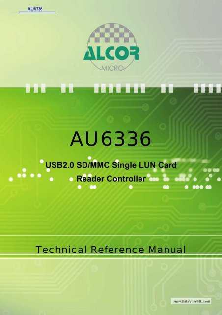
AU6336 USB2.0 SD/MMC Single LUN Card Reader Controller
AU6336 USB2.0 SD/MMC Single LUN Card Reader Controller
AU6336 USB2.0 SD/MMC Single LUN Card Reader Controller

You also want an ePaper? Increase the reach of your titles
YUMPU automatically turns print PDFs into web optimized ePapers that Google loves.
www.DataSheet4U.com<br />
<strong>AU6336</strong><br />
<strong>USB2.0</strong> <strong>SD</strong>/<strong>MMC</strong> <strong>Single</strong> <strong>LUN</strong> <strong>Card</strong><br />
<strong>Reader</strong> <strong>Controller</strong>
www.DataSheet4U.com<br />
Copyright<br />
Copyright © 1997 - 2007. Alcor Micro, Corp. All Rights Reserved. No part of this data<br />
sheet may be reproduced, transmitted, transcribed, stored in a retrieval system or<br />
translated into any language or computer language, in any form or by any means,<br />
electronic, mechanical, magnetic, optical, chemical, manual or otherwise, without prior<br />
written permission from Alcor Micro, Corp.<br />
Trademark Acknowledgements<br />
The company and product names mentioned in this document may be the trademarks<br />
or registered trademarks of their manufacturers.<br />
Disclaimer<br />
Alcor Micro, Corp. reserves the right to change this product without prior notice. Alcor<br />
Micro, Corp. makes no warranty for the use of its products and bears no responsibility<br />
for any error that appear in this document. Specifications are subject to change<br />
without prior notice.<br />
Revision History<br />
Date Revision Description<br />
Aug 2007 0.9W Preliminary Release.<br />
Oct 2007 1.00W Official Release<br />
Contact Information:<br />
Web site: http://www.alcormicro.com/<br />
Taiwan China ShenZhen Office<br />
Alcor Micro, Corp. Rm.2407-08, Industrial Bank Building<br />
4F, No 200 Kang Chien Rd., Nei Hu, No.4013, Shennan Road,<br />
Taipei, Taiwan, R.O.C. ShenZhen,China. 518026<br />
Phone: 886-2-8751-1984 Phone: (0755) 8366-9039<br />
Fax: 886-2-2659-7723 Fax: (0755) 8366-9101<br />
Santa Clara Office Los Angeles Office<br />
2901 Tasman Drive, Suite 206 9070 Rancho Park Court<br />
Santa Clara, CA 95054 Rancho Cucamonga, CA 91730<br />
USA USA<br />
Phone: (408) 845-9300 Phone: (909) 483-8821<br />
Fax: (408) 845-9086 Fax: (909) 944-0464
www.DataSheet4U.com<br />
www.DataSheet4U.com<br />
Table of Contents<br />
1. Introduction ............................................................ 1<br />
1.1 Description...................................................................................1<br />
1.2 Features........................................................................................1<br />
2. Application Block Diagram ................................... 2<br />
3. Pin Assignment ...................................................... 3<br />
4. System Architecture and Reference Design ....... 7<br />
4.1 <strong>AU6336</strong> Block Diagram ...............................................................7<br />
5. Electrical Characteristics ...................................... 8<br />
5.1 Absolute Maximum Ratings........................................................8<br />
5.2 Recommended Operating Conditions .......................................8<br />
5.3 General DC Characteristics ........................................................8<br />
5.4 DC Electrical Characteristics of 3.3V I/O Cells..........................9<br />
5.5 USB Transceiver Characteristics ...............................................9<br />
5.6 Power Switch Feature .................................................................13<br />
6. Mechanical Information ......................................... 14<br />
7. Abbreviations ......................................................... 16<br />
i
www.DataSheet4U.com<br />
List of Figures<br />
ii<br />
Figure 2.1 Block Diagram..................................................................2<br />
Figure 3.1 <strong>AU6336</strong>-MAS Pin Assignment Diagram .........................3<br />
Figure 3.2 <strong>AU6336</strong>-MDF Pin Assignment Diagram .........................5<br />
Figure 4.1 <strong>AU6336</strong> Block Diagram ...................................................7<br />
Figure 5.1 <strong>Card</strong> Detect Power-in Timing..........................................13<br />
Figure 6.1 28 SSOP Mechanical Information Diagram ...................14<br />
Figure 6.2 24 QFN Mechanical Information Diagram......................15<br />
List of Tables<br />
Table 3.1 <strong>AU6336</strong>-MAS Pin Descriptions.........................................4<br />
Table 3.2 <strong>AU6336</strong>-MDF Pin Descriptions.........................................6<br />
Table 5.1 Absolute Maximum Ratings .............................................8<br />
Table 5.2 Recommended Operating Conditions .............................8<br />
Table 5.3 General DC Characteristics..............................................8<br />
Table 5.4 DC Electrical Characteristics of 3.3V I/O Cells ...............9<br />
Table 5.5 Electrical characteristics ..................................................9<br />
Table 5.6 Static characteristic:Digital pin .....................................10<br />
Table 5.7 Static characteristic:Analog I/O pins(DP/DM)..........10<br />
Table 5.8 Dynamic characteristic:Analog I/O pins(DP/DM).....11
www.DataSheet4U.com<br />
1. Introduction<br />
1.1 Description<br />
<strong>AU6336</strong> is an <strong>USB2.0</strong> high-speed transmission controller, which is designed as a<br />
bridge between USB and <strong>SD</strong> compatible flash card interface, such as <strong>SD</strong>, HS-<strong>SD</strong>,<br />
<strong>MMC</strong>, HS-<strong>MMC</strong>, RS-<strong>MMC</strong>, <strong>MMC</strong>micro…etc. <strong>AU6336</strong> can read digital contents stored<br />
on memory card designed to cover a wide area of applications such as digital<br />
cameras, PDAs, MP3 players and smart phones…etc.<br />
<strong>AU6336</strong> inherits the high-performance and cost-efficiency character from Alcor’s<br />
products, included power switch integration, dynamic icon utility support, and DMA<br />
engine integration.<br />
1.2 Features<br />
� Support USB V2.0 specification and USB Device Class Definition for Mass<br />
Storage, Bulk-Transport V1.0<br />
� Support <strong>SD</strong>/<strong>MMC</strong> compatible flash card<br />
� Support the latest flash card specification: <strong>SD</strong>2.0 (<strong>SD</strong>HC), MSPro parallel<br />
mode (4-bit)<br />
� Alcor DMA engine integrated for performance enhancement<br />
� Work with default driver from Windows ME/2000/XP/Vista and Mac OS X;<br />
Windows 98/2000(SP1/SP2) and Mac OS 9 are supported by vendor driver<br />
from Alcor.<br />
� Compliant to xD 1.2 spec.<br />
� Ping-pong FIFO implementation for concurrent bus operation.<br />
� Support multiple sectors transfer optimize performance<br />
� Support Dynamic Icon Utility<br />
� Support LED for bus operating indication<br />
� Power switch integrated to reduce production BOM cost<br />
� 5�3.3 and 3.3�1.8V regulators built in<br />
� 28-SSOP package for <strong>SD</strong>/<strong>MMC</strong><br />
� 24-QFN package for <strong>SD</strong>/<strong>MMC</strong><br />
<strong>AU6336</strong> <strong>USB2.0</strong> <strong>SD</strong>/<strong>MMC</strong> <strong>Single</strong> <strong>LUN</strong> <strong>Card</strong> <strong>Reader</strong> <strong>Controller</strong> V1.00W 1
www.DataSheet4U.com<br />
2. Application Block Diagram<br />
Following application diagram demonstrates a typical card reader using the <strong>AU6336</strong><br />
chip. By connecting the card reader to a desktop or notebook PC through USB bus,<br />
the <strong>AU6336</strong> becomes a bus-powered, high speed USB card reader, which can be<br />
used as a bridge for data transfer between Desktop PC and Notebook PC.<br />
2<br />
Figure 2.1 Block Diagram<br />
PC with USB Host <strong>Controller</strong><br />
<strong>AU6336</strong><br />
<strong>SD</strong>/<strong>MMC</strong><br />
Digital Camera<br />
MP3 Player<br />
PDA<br />
Moble Phones<br />
<strong>AU6336</strong> <strong>USB2.0</strong> <strong>SD</strong>/<strong>MMC</strong> <strong>Single</strong> <strong>LUN</strong> <strong>Card</strong> <strong>Reader</strong> V1.00W<br />
PC
www.DataSheet4U.com<br />
3. Pin Assignment<br />
There are two different form factor packages available to choose from. The following<br />
figure shows signal names for each pin and the table in the page after describes each<br />
pin in details.<br />
Figure 3.1 <strong>AU6336</strong>-MAS Pin Assignment Diagram<br />
GPI4<br />
GND<br />
VDD<br />
REXT<br />
VD33P<br />
DP<br />
DM<br />
VS33P<br />
XI<br />
XO<br />
VDDU<br />
AGND5V<br />
AVDD5V<br />
VDD3V<br />
1<br />
2<br />
3<br />
4<br />
5<br />
6<br />
7<br />
8<br />
9<br />
10<br />
11<br />
12 17<br />
13<br />
14<br />
Alcor Micro<br />
<strong>AU6336</strong>-MAS<br />
28-PIN SSOP<br />
<strong>AU6336</strong> <strong>USB2.0</strong> <strong>SD</strong>/<strong>MMC</strong> <strong>Single</strong> <strong>LUN</strong> <strong>Card</strong> <strong>Reader</strong> <strong>Controller</strong> V1.00W 3<br />
28<br />
27<br />
26<br />
25<br />
24<br />
23<br />
22<br />
21<br />
20<br />
19<br />
18<br />
16<br />
15<br />
<strong>SD</strong>CLK<br />
<strong>SD</strong>DATA0<br />
<strong>SD</strong>DATA3<br />
CLED<br />
<strong>SD</strong>DATA2<br />
<strong>SD</strong>WP<br />
<strong>SD</strong>DATA1<br />
<strong>SD</strong>CMD<br />
<strong>SD</strong>_V33<br />
VDD33C<br />
<strong>SD</strong>CDN<br />
VSSHM<br />
VDDHM<br />
V18
www.DataSheet4U.com<br />
4<br />
Table 3.1 <strong>AU6336</strong>-MAS Pin Descriptions<br />
Pin # Pin Name I/O Description<br />
1 GPI4 I<br />
Force to full speed<br />
'1' for normal [default]<br />
'0' for force to full speed.<br />
2 GND I Core ground<br />
3 VDD I Core 1.8V power input<br />
4 REXT I UTMI reference resistor<br />
5 VD33P I UTMI 3.3V power input<br />
6 DP I/O USB DP<br />
7 DM I/O USB DM<br />
8 VS33P I UTMI 3.3V ground<br />
9 XI I 12MHz crystal input<br />
10 XO O 12MHz crystal output<br />
11 VDDU I UTMI 1.8V input<br />
12 AGND5V I 5 to 3.3 regulator ground<br />
13 AVDD5V I 5 to 3.3 regulator 5V input<br />
14 VDD3V O 5 to 3.3 regulator 3.3V output<br />
15 V18 I 3.3 to 1.8 regulator 1.8V output<br />
16 VDDHM I IO 3.3V power / 3.3 to 1.8 regulator 3.3V input<br />
17 VSSHM I IO 3.3V ground<br />
18 <strong>SD</strong>CDN I <strong>SD</strong> card detect<br />
19 VDD33C I <strong>Card</strong> power switch 3.3V input<br />
20 <strong>SD</strong>_V33 O <strong>Card</strong> power switch output<br />
21 <strong>SD</strong>CMD I/O <strong>SD</strong> command<br />
22 <strong>SD</strong>DATA1 I/O <strong>SD</strong> data 1<br />
23 <strong>SD</strong>WP I <strong>SD</strong> write protect<br />
24 <strong>SD</strong>DATA2 I/O <strong>SD</strong> data 2<br />
25 CLED O <strong>Card</strong> Access LED<br />
26 <strong>SD</strong>DATA3 I/O <strong>SD</strong> data 3<br />
27 <strong>SD</strong>DATA0 I/O <strong>SD</strong> data 0<br />
28 <strong>SD</strong>CLK O <strong>SD</strong> clock<br />
<strong>AU6336</strong> <strong>USB2.0</strong> <strong>SD</strong>/<strong>MMC</strong> <strong>Single</strong> <strong>LUN</strong> <strong>Card</strong> <strong>Reader</strong> V1.00W
www.DataSheet4U.com<br />
The following figure shows signal names of each pin of the 24 QFN package and the<br />
table in the page after describes each pin in details.<br />
VD33P<br />
DP<br />
DM<br />
VS33P<br />
XI<br />
XO<br />
Figure 3.2 <strong>AU6336</strong>-MDF Pin Assignment Diagram<br />
1<br />
2<br />
3<br />
4<br />
5<br />
6<br />
REXT<br />
24<br />
23<br />
22 21 20 19<br />
ALCOR MICRO<br />
<strong>AU6336</strong><br />
24PIN QFN<br />
7 8 9 10 11 12<br />
VDDU<br />
VDD<br />
AVDD5V<br />
<strong>SD</strong>CLK<br />
VDD3V<br />
<strong>AU6336</strong> <strong>USB2.0</strong> <strong>SD</strong>/<strong>MMC</strong> <strong>Single</strong> <strong>LUN</strong> <strong>Card</strong> <strong>Reader</strong> <strong>Controller</strong> V1.00W 5<br />
<strong>SD</strong>DATA0<br />
V18<br />
<strong>SD</strong>DATA3<br />
VDDHM<br />
CLED<br />
<strong>SD</strong>CDN<br />
18<br />
17<br />
16<br />
15<br />
14<br />
13<br />
<strong>SD</strong>DATA2<br />
<strong>SD</strong>WP<br />
<strong>SD</strong>DATA1<br />
<strong>SD</strong>CMD<br />
<strong>SD</strong>_V33<br />
VDD33C
www.DataSheet4U.com<br />
6<br />
Table 3.2 <strong>AU6336</strong>-MDF Pin Descriptions<br />
Pin # Pin Name I/O Description<br />
1 VD33P I UTMI 3.3V power input<br />
2 DP I/O USB DP<br />
3 DM I/O USB DM<br />
4 VS33P I UTMI 3.3V ground<br />
5 XI I 12MHz crystal input<br />
6 XO O 12MHz crystal output<br />
7 VDDU I UTMI 1.8V input<br />
8 AVDD5V I 5 to 3.3 regulator 5V input<br />
9 VDD3V O<br />
5V to 3.3V regulator 3.3V output<br />
3.3V to 1.8V regulator 3.3V input<br />
10 V18 O 3.3V to 1.8V regulator 1.8V output<br />
11 VDDHM I IO 3.3V power / 3.3 to 1.8 regulator 3.3V input<br />
12 <strong>SD</strong>CDN I <strong>SD</strong> card detect<br />
13 VDD33C I <strong>Card</strong> power switch 3.3V input<br />
14 <strong>SD</strong>_V33 O <strong>Card</strong> power switch output<br />
15 <strong>SD</strong>CMD I/O <strong>SD</strong> command<br />
16 <strong>SD</strong>DATA1 I/O <strong>SD</strong> data 1<br />
17 <strong>SD</strong>WP I <strong>SD</strong> write protect<br />
18 <strong>SD</strong>DATA2 I/O <strong>SD</strong> data 2<br />
19 CLED O<br />
20 <strong>SD</strong>DATA3 I/O <strong>SD</strong> data 3<br />
21 <strong>SD</strong>DATA0 I/O <strong>SD</strong> data 0<br />
22 <strong>SD</strong>CLK O <strong>SD</strong> clock<br />
<strong>Card</strong> access LED.<br />
Low for card present<br />
High for card absent<br />
Blink for card access<br />
23 VDD I Core 1.8V power input<br />
24 REXT I UTMI reference resistor<br />
<strong>AU6336</strong> <strong>USB2.0</strong> <strong>SD</strong>/<strong>MMC</strong> <strong>Single</strong> <strong>LUN</strong> <strong>Card</strong> <strong>Reader</strong> V1.00W
www.DataSheet4U.com<br />
USB<br />
Upstream<br />
Port<br />
4. System Architecture and Reference<br />
Design<br />
4.1 <strong>AU6336</strong> Block Diagram<br />
XCVR<br />
1.8 V<br />
3.3V/1.8V<br />
Voltage<br />
Regulator<br />
Figure 4.1 <strong>AU6336</strong> Block Diagram<br />
Processor<br />
USB<br />
SIE<br />
ROM<br />
RAM<br />
Arbitrator<br />
12MHz<br />
XTAL 5V<br />
<strong>SD</strong>/<strong>MMC</strong><br />
Control FIFO<br />
5V→3.3V<br />
Regulator<br />
3.3V<br />
Power<br />
Switch<br />
<strong>SD</strong><br />
<strong>MMC</strong><br />
<strong>AU6336</strong> <strong>USB2.0</strong> <strong>SD</strong>/<strong>MMC</strong> <strong>Single</strong> <strong>LUN</strong> <strong>Card</strong> <strong>Reader</strong> <strong>Controller</strong> V1.00W 7<br />
<strong>SD</strong>/<strong>MMC</strong> PWR
www.DataSheet4U.com<br />
5. Electrical Characteristics<br />
5.1 Absolute Maximum Ratings<br />
Table 5.1 Absolute Maximum Ratings<br />
SYMBOL PARAMETER RATING UNITS<br />
VDDHM Power Supply -0.3 to VDDH +0.3 V<br />
VIN Input Signal Voltage -0.3 to 3.6 V<br />
VOUT Output Signal Voltage -0.3 to VDDHM +0.3 V<br />
TSTG Storage Temperature -40 to 150<br />
5.2 Recommended Operating Conditions<br />
Table 5.2 Recommended Operating Conditions<br />
SYMBOL PARAMETER MIN TYP MAX UNITS<br />
VDDHM Power Supply 3.0 3.3 3.6 V<br />
V18 Digital Supply 1.62 1.8 1.98 V<br />
VIN Input Signal Voltage 0 3.3 3.6 V<br />
TOPR Operating Temperature 0 85<br />
5.3 General DC Characteristics<br />
Table 5.3 General DC Characteristics<br />
SYMBOL PARAMETER CONDITIONS MIN TYP MAX UNITS<br />
8<br />
IIN<br />
Input current<br />
No pull-up or<br />
pull-down<br />
O C<br />
O C<br />
-10 ±1 10 µA<br />
IOZ Tri-state leakage current -10 ±1 10 µA<br />
CIN Input capacitance Pad Limit 2.8 ρF<br />
COUT Output capacitance Pad Limit 2.8 ρF<br />
CBID<br />
Bi-directional buffer<br />
capacitance<br />
Pad Limit 2.8 ρF<br />
<strong>AU6336</strong> <strong>USB2.0</strong> <strong>SD</strong>/<strong>MMC</strong> <strong>Single</strong> <strong>LUN</strong> <strong>Card</strong> <strong>Reader</strong> V1.00W
www.DataSheet4U.com<br />
5.4 DC Electrical Characteristics of 3.3V I/O Cells<br />
Table 5.4 DC Electrical Characteristics of 3.3V I/O Cells<br />
Limits<br />
SYMBOL PARAMETER CONDITIONS MIN TYP MAX UNIT<br />
VDDHM Power supply 3.3V I/O 3.0 3.3 3.6 V<br />
Vil Input low voltage 0.8 V<br />
LVTTL<br />
Input high voltage<br />
2.0 V<br />
Vih<br />
Vol Output low voltage ∣Iol∣=2~16mA 0.4 V<br />
Voh Output high voltage ∣Ioh∣=2~16mA 2.4 V<br />
Rpu Input pull-up resistance PU=high, PD=low 55 75 110 KΩ<br />
Rpd Input pull-down resistance PU=low, PD=high 40 75 150 KΩ<br />
Iin Input leakage current Vin= VDDHM or 0 -10 ±1 10 μA<br />
Ioz<br />
Tri-state output leakage<br />
current<br />
5.5 USB Transceiver Characteristics<br />
Table 5.5 Electrical characteristics<br />
-10 ±1 10 μA<br />
Symbol Parameter Conditions Min. Typ. Max. Unit<br />
VDD33 Analog supply Voltage 3.0 3.3 3.6 V<br />
V18 Digital supply Voltage 1.62 1.8 1.98 V<br />
ICC<br />
Operating supply current<br />
High speed operating<br />
at 480 MHz<br />
55 mA<br />
<strong>AU6336</strong> <strong>USB2.0</strong> <strong>SD</strong>/<strong>MMC</strong> <strong>Single</strong> <strong>LUN</strong> <strong>Card</strong> <strong>Reader</strong> <strong>Controller</strong> V1.00W 9
www.DataSheet4U.com<br />
Table 5.6 Static characteristic:Digital pin<br />
Symbol Parameter Conditions Min. Typ. Max. Unit<br />
Input levels<br />
VIL Low-level input voltage 0.8 V<br />
VIH High-level input voltage 2.0 V<br />
Output levels<br />
VOL Low-level output voltage 0.2 V<br />
VOH High-level output voltage VDDH-0.2 V<br />
Table 5.7 Static characteristic:Analog I/O pins(DP/DM)<br />
Symbol Parameter Conditions<br />
<strong>USB2.0</strong> Transceiver(HS)<br />
Min. Typ. Max. Unit<br />
Input Levels(differential receiver)<br />
VH<strong>SD</strong>IFF<br />
VHSCM<br />
VHSSQ<br />
VH<strong>SD</strong>SC<br />
VHSOI<br />
VHSOL<br />
VHSOH<br />
VCHIRPJ<br />
VCHIRPK<br />
RDRV<br />
10<br />
High speed differential<br />
input sensitivity<br />
High speed data signaling<br />
common mode voltage<br />
range<br />
∣VI (DP )-VI (DM )∣<br />
measured at the<br />
connection as<br />
application circuit<br />
300 mV<br />
-50 500 mV<br />
High speed squelch Squelch detected 100 mV<br />
detection threshold No squelch detected 150 mV<br />
Disconnection<br />
High speed disconnection detected<br />
detection threshold Disconnection not<br />
detected<br />
Output Levels<br />
High speed idle level<br />
output voltage(differential)<br />
High speed low level<br />
output voltage(differential)<br />
High speed high level<br />
output voltage(differential)<br />
Chirp-J output voltage<br />
(differential)<br />
Chirp-K output voltage<br />
(differential)<br />
Resistance<br />
Equivalent resistance<br />
Driver output impedance used as internal chip<br />
only<br />
625 mV<br />
525 mV<br />
-10 10 mV<br />
-10 10 mV<br />
-360 400 mV<br />
700 1100 mV<br />
-900 -500 mV<br />
3 6 9 Ω<br />
<strong>AU6336</strong> <strong>USB2.0</strong> <strong>SD</strong>/<strong>MMC</strong> <strong>Single</strong> <strong>LUN</strong> <strong>Card</strong> <strong>Reader</strong> V1.00W
www.DataSheet4U.com<br />
VTERM<br />
VDI<br />
VCM<br />
VSE<br />
Termination voltage for<br />
pull-up resistor on pin<br />
RPU<br />
Overall resistance<br />
including external<br />
resistor<br />
Termination<br />
40.5 45 49.5<br />
3.0 3.6 V<br />
USB1.1 Transceiver(FS/LS)<br />
Input Levels(differential receiver)<br />
Differential input<br />
sensitivity<br />
∣VI (DP )-VI (DM )∣ 0.2 V<br />
Differential common<br />
mode voltage<br />
0.8 2.5 V<br />
Input Levels(single-ended receivers)<br />
<strong>Single</strong> ended receiver<br />
threshold<br />
0.8 2.0 V<br />
Output levels<br />
VOL Low-level output voltage 0 0.3 V<br />
VOH High-level output voltage 2.8 3.6 V<br />
Table 5.8 Dynamic characteristic:Analog I/O pins(DP/DM)<br />
Symbol Parameter Conditions Min. Typ. Max. Unit<br />
tHSR<br />
tHSF<br />
tFR<br />
tFF<br />
tFRMA<br />
VCRS<br />
tLR<br />
High-speed differential<br />
rise time<br />
High-speed differential fall<br />
time<br />
Rise time<br />
Fall time<br />
Differential rise/fall time<br />
matching(tFR / tFF)<br />
Output signal crossover<br />
voltage<br />
Rise time<br />
Driver Characteristics<br />
High-Speed Mode<br />
Full-Speed Mode<br />
CL=50pF;10 to 90%<br />
of∣VOH-VOL∣;<br />
CL=50pF;90 to 10%<br />
of∣VOH-VOL∣;<br />
Excluding the first<br />
transition from idle<br />
mode<br />
Excluding the first<br />
transition from idle<br />
mode<br />
Low-Speed Mode<br />
CL=200pF-600pF;<br />
10 to 90%of<br />
∣VOH-VOL∣;<br />
500 ps<br />
500 ps<br />
4 20 ns<br />
4 20 ns<br />
90 110 %<br />
1.3 2.0 V<br />
75 300 ns<br />
<strong>AU6336</strong> <strong>USB2.0</strong> <strong>SD</strong>/<strong>MMC</strong> <strong>Single</strong> <strong>LUN</strong> <strong>Card</strong> <strong>Reader</strong> <strong>Controller</strong> V1.00W 11
www.DataSheet4U.com<br />
tLF<br />
tLRMA<br />
VCRS<br />
Fall time<br />
Differential rise/fall time<br />
matching(tLR / tLF)<br />
Output signal crossover<br />
voltage<br />
CL=200pF-600pF;<br />
90 to 10%of<br />
∣VOH-VOL∣;<br />
Excluding the first<br />
transition from idle<br />
mode<br />
Excluding the first<br />
transition from idle<br />
mode<br />
75 300 ns<br />
80 125 %<br />
1.3 2.0 V<br />
VOH High-level output voltage 2.8 3.6 V<br />
12<br />
<strong>AU6336</strong> <strong>USB2.0</strong> <strong>SD</strong>/<strong>MMC</strong> <strong>Single</strong> <strong>LUN</strong> <strong>Card</strong> <strong>Reader</strong> V1.00W
www.DataSheet4U.com<br />
5.6 Power Switch Feature<br />
CARD_POWER<br />
CARD_DETECT<br />
100ms + System<br />
Polling timing<br />
Figure 5.1 <strong>Card</strong> Detect Power-in Timing<br />
1ms to 10ms ( Depend<br />
Load Capacitor )<br />
3.3V+/- 0.3V<br />
<strong>AU6336</strong> <strong>USB2.0</strong> <strong>SD</strong>/<strong>MMC</strong> <strong>Single</strong> <strong>LUN</strong> <strong>Card</strong> <strong>Reader</strong> <strong>Controller</strong> V1.00W 13
www.DataSheet4U.com<br />
6. Mechanical Information<br />
14<br />
Figure 6.1 28 SSOP Mechanical Information Diagram<br />
<strong>AU6336</strong> <strong>USB2.0</strong> <strong>SD</strong>/<strong>MMC</strong> <strong>Single</strong> <strong>LUN</strong> <strong>Card</strong> <strong>Reader</strong> V1.00W
www.DataSheet4U.com<br />
Figure 6.2 24 QFN Mechanical Information Diagram<br />
<strong>AU6336</strong> <strong>USB2.0</strong> <strong>SD</strong>/<strong>MMC</strong> <strong>Single</strong> <strong>LUN</strong> <strong>Card</strong> <strong>Reader</strong> <strong>Controller</strong> V1.00W 15
www.DataSheet4U.com<br />
7. Abbreviations<br />
In this chapter some of the terms and abbreviations used throughout the technical<br />
reference manual are listed as follows.<br />
SIE Serial Interface Engine<br />
<strong>SD</strong> Secure Digital<br />
<strong>MMC</strong> Multimedia <strong>Card</strong><br />
UTMI USB Transceiver Macrocell Interface<br />
About Alcor Micro, Corp.<br />
Alcor Micro, Corp. designs, develops and markets highly integrated and advanced<br />
peripheral semiconductor, and software driver solutions for the personal computer<br />
and consumer electronics markets worldwide. We specialize in USB solutions and<br />
focus on emerging technology such as USB and IEEE 1394. The company offers a<br />
range of semiconductors including controllers for USB hub, integrated keyboard/USB<br />
hub and USB Flash memory card reader…etc. Alcor Micro, Corp. is based in Taipei,<br />
Taiwan, with sales offices in Taipei, Japan, Korea and California. Alcor Micro is<br />
distinguished by its ability to provide innovative solutions for spec-driven products.<br />
Innovations like single chip solutions for traditional multiple chip products and<br />
on-board voltage regulators enable the company to provide cost-efficiency solutions<br />
for the computer peripheral device OEM customers worldwide.<br />
16<br />
<strong>AU6336</strong> <strong>USB2.0</strong> <strong>SD</strong>/<strong>MMC</strong> <strong>Single</strong> <strong>LUN</strong> <strong>Card</strong> <strong>Reader</strong> V1.00W