Device simulation - Silvaco International
Device simulation - Silvaco International
Device simulation - Silvaco International

Create successful ePaper yourself
Turn your PDF publications into a flip-book with our unique Google optimized e-Paper software.
<strong>Device</strong> <strong>simulation</strong><br />
Maria Concetta Allia
IMS CAD & Design Services<br />
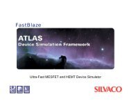
Atlas overview<br />
Atlas is a physically-based two and three dimensional device simulator that<br />
predicts the electrical behavior of semiconductor devices at specified bias conditions.<br />
The physical structures simulated with Athena are used as input by Atlas.<br />
The combination of Athena and Atlas makes possible to determine the impact of<br />
process parameters on device characteristics.<br />
Atlas input file<br />
It is a text file that can be arranged<br />
by using Deckbuild or any text editor.<br />
It collects a sequence of commands<br />
(statements) corresponding to required<br />
bias conditions and control commands<br />
specified to select physical models and<br />
parameters.<br />
Maria Concetta Allia<br />
Atlas <strong>simulation</strong><br />
Generating Atlas input file<br />
Running Atlas <strong>simulation</strong><br />
Analyzing Atlas output file<br />
<strong>Device</strong><br />
2
IMS CAD & Design Services<br />
Simulation problem specification<br />
The <strong>simulation</strong> problem must be specified in the input file, defining the<br />
following steps:<br />
The physical structure to be simulated.<br />
The physical models to be used.<br />
The numerical methods needed to solve the physical equations.<br />
The bias conditions for the electrical characteristics.<br />
The present section describes how to perform these steps.<br />
Maria Concetta Allia<br />
<strong>Device</strong><br />
3
Running Atlas inside Deckbuild<br />
IMS CAD & Design Services<br />
Running Atlas <strong>simulation</strong><br />
To run Atlas inside Deckbuild use the<br />
following command line:<br />
> go atlas<br />
Running a given Atlas version<br />
The syntax is:<br />
> go atlas simflags=“-V 5.10.0.R”<br />
Running Atlas without Deckbuild<br />
To run Atlas directly under unix use the<br />
following command line:<br />
> atlas <br />
> atlas –V 5.10.0.R <br />
Maria Concetta Allia<br />
<strong>Device</strong><br />
4
Atlas uses two types of input file<br />
A text file that contains Atlas<br />
commands.<br />
A structure file that defines the<br />
structure to be simulated<br />
ATHENA<br />
DEVEDIT<br />
DECKBUILD<br />
IMS CAD & Design Services<br />
Atlas Inputs and Outputs<br />
Structure File<br />
ATLAS<br />
Command File<br />
Atlas produces three types of output files<br />
The runtime output that gives error and<br />
warning messages as the <strong>simulation</strong> proceeds.<br />
The log file that stores voltages and currents.<br />
The structure file that stores 2D and 3D data<br />
relating to the values of solution variables<br />
Runtime Output<br />
Log File<br />
Structure File<br />
Maria Concetta Allia<br />
TONYPLOT<br />
<strong>Device</strong><br />
5
IMS CAD & Design Services<br />
Atlas input structure<br />
The physical structure built by Athena is used as input by Atlas to predict its<br />
electrical behavior. The grid of the input structure is crucial for the device <strong>simulation</strong>.<br />
There is a trade-off between<br />
the requirements of accuracy<br />
and numerical efficiency<br />
Maria Concetta Allia<br />
Accuracy requires a fine grid<br />
Numerical efficiency is greater<br />
when fewer grid points are used<br />
The most efficient way to work is to allocate a fine grid only in critical areas and<br />
a coarser grid elsewhere. Most critical areas tend to coincide with reverse biased<br />
metallurgical junctions.<br />
Typical critical areas<br />
Transverse electric field under the MOSFET gate<br />
Areas of considerable recombination effects<br />
Areas of high impact ionization<br />
<strong>Device</strong><br />
6
An Atlas input file is:<br />
IMS CAD & Design Services<br />
Question 1<br />
a) a text file that contains Atlas commands<br />
b) a log file that stores voltages and currents<br />
c) a structure file that contains Atlas commands<br />
Maria Concetta Allia<br />
<strong>Device</strong><br />
7
Usually, a grid that is appropriate<br />
for process <strong>simulation</strong> is not always<br />
appropriate for device <strong>simulation</strong>.<br />
Before<br />
remeshing<br />
8000 nodes<br />
IMS CAD & Design Services<br />
Devedit<br />
After<br />
remeshing<br />
3500 nodes<br />
Maria Concetta Allia<br />
To remesh the process <strong>simulation</strong><br />
output for device <strong>simulation</strong>, the<br />
structure editing end griding tool<br />
Devedit can be used.<br />
The Standard Structure File<br />
can be read into Devedit.<br />
The mesh contained into<br />
the file can be replaced using<br />
the meshbuild algorithm.<br />
The mesh can be refined by<br />
setting parameters that<br />
describe critical areas or by<br />
simply pointing to the areas<br />
that require refinement.<br />
<strong>Device</strong><br />
8
IMS CAD & Design Services<br />
Remeshing<br />
When remeshing a structure for device <strong>simulation</strong><br />
Ensure adequate mesh density in high field areas<br />
Avoid abrupt discontinuities in mesh density<br />
Avoid, or at least minimize, the number of obtuse triangles<br />
Avoid, or at least minimize, the number of long and thin triangles<br />
Atlas sets some limits on the maximum number of grid nodes<br />
2D Atlas <strong>simulation</strong>s have a maximum node limit of 20,000. This limit is high<br />
enough for <strong>simulation</strong>s of conventional devices.<br />
For most 2D <strong>simulation</strong>s, you can obtain accurate results with somewhere<br />
between 6,000 and 10,000 node points properly located in the structure.<br />
Maria Concetta Allia<br />
<strong>Device</strong><br />
9
IMS CAD & Design Services<br />
Question 2<br />
When remeshing a structure for device <strong>simulation</strong>, ensure:<br />
a) an adequate number of obtuse triangles<br />
b) a number of nodes greater than 20,000<br />
c) an adequate mesh density in critical areas<br />
Maria Concetta Allia<br />
<strong>Device</strong><br />
10
IMS CAD & Design Services<br />
Atlas output: structure files<br />
Structure files (.str) provide an image of the device at a particular bias point. This<br />
allows to display any evaluated quantity within the device structure, from doping<br />
profiles and band parameters to electron concentrations and electric fields.<br />
Structure files can be plotted using<br />
Tonyplot.<br />
Several quantities are saved by default<br />
within the structure file (doping, electron<br />
concentration, potential, electric field).<br />
Additional quantities can be specified by<br />
using the OUTPUT statement.<br />
Maria Concetta Allia<br />
<strong>Device</strong><br />
11
IMS CAD & Design Services<br />
Atlas output: log files<br />
Log files (.log) store the terminal characteristics calculated by Atlas. These are<br />
current and voltages at electrodes in DC <strong>simulation</strong>s. In transient <strong>simulation</strong>s, the time<br />
is stored. In AC <strong>simulation</strong>s, the small signal frequency, the conductances and<br />
capacitances are saved.<br />
Log files can be plotted using Tonyplot.<br />
The statement LOG OUTF= is used<br />
to open a log file. Terminal characteristics from<br />
all SOLVE statements after the LOG statement<br />
are saved into this file. To not save the terminal<br />
characteristics to this file, use the LOG OFF<br />
statement.<br />
A separate log file should be used for each<br />
bias sweep. For example, separate log files<br />
are used for each gate bias in a MOS Id/Vds<br />
<strong>simulation</strong> or for each base current in a bipolar<br />
Ic/Vce <strong>simulation</strong>. These files can be overlaid in<br />
Tonyplot.<br />
Maria Concetta Allia<br />
<strong>Device</strong><br />
12
Atlas structure output:<br />
IMS CAD & Design Services<br />
Question 3<br />
a) can be plotted using Tecplot<br />
b) stores currents and voltages at electrodes<br />
c) saves quantities as electron concentration, potential,<br />
electric field at a particular bias point<br />
Maria Concetta Allia<br />
<strong>Device</strong><br />
13
IMS CAD & Design Services<br />
Extract function<br />
The Extract command (provided within the Deckbuild environment) allows to extract<br />
device parameters, operating on the log file or the structure file. To generate the<br />
Extract statement:<br />
Select Extract → <strong>Device</strong>… from the Commands menu<br />
In the Extraction popup a list of ready-made extract statements is provided<br />
The User defined option allows to generate custom extracts<br />
Maria Concetta Allia<br />
It is possible to create<br />
customized expressions or<br />
choose from a number of<br />
standard routines provided for<br />
the device simulators.<br />
It is also possible to take one of the standard expressions and<br />
to modify it to suit needs.<br />
<strong>Device</strong><br />
14
IMS CAD & Design Services<br />
Atlas examples<br />
Atlas examples are a good starting point for creating a device <strong>simulation</strong>. It is<br />
possible to access the examples through Deckbuild:<br />
Click on the Main Control menu<br />
Select Examples:<br />
the examples are divided by technology or technology group<br />
Choose the technology by double clicking over that item:<br />
a list of examples for that technology will appear<br />
Choose a particular example by double clicking over that item in the list:<br />
a text description of the example will appear in the window<br />
Press the Load Example button:<br />
the input command file will be loaded into Deckbuild<br />
Press the Run button to run the example<br />
Maria Concetta Allia<br />
<strong>Device</strong><br />
15
IMS CAD & Design Services<br />
Basic Semiconductor Equations<br />
The mathematical model that describes semiconductor device physics consists<br />
of a set of fundamental equations (derived from Maxwell’s laws), which link<br />
together electrostatic potential and carriers densities:<br />
Poisson’s equation<br />
Continuity equation<br />
Constitutive equation<br />
It relates variations in electrostatic<br />
potential to local charge densities.<br />
They describe the way electron<br />
and hole densities evolve as a<br />
result of transport, generation, and<br />
recombination processes.<br />
Maria Concetta Allia<br />
<strong>Device</strong><br />
16
It relates variations in electrostatic potential to space charge densities:<br />
where:<br />
ψ is the electrostatic potential<br />
ε is the local permittivity<br />
ρ is the local space charge density<br />
The local space charge density is the sum of contributions from all mobile<br />
and fixed charges, including electrons, holes, and ionized impurities.<br />
IMS CAD & Design Services<br />
Poisson’s equation<br />
div(<br />
ε ∇ ψ ) = −ρ<br />
The electric field is obtained from the gradient of the potential:<br />
E<br />
= -∇ψ<br />
Maria Concetta Allia<br />
<strong>Device</strong><br />
17
The continuity equations for electrons and holes are defined by:<br />
where:<br />
IMS CAD & Design Services<br />
Carrier continuity equation<br />
∂n<br />
1<br />
− div J<br />
∂t<br />
q<br />
∂p<br />
1<br />
+ div J<br />
∂t<br />
q<br />
n<br />
p<br />
= G<br />
= G<br />
n and p are the electron and hole concentration<br />
J<br />
G<br />
R<br />
n<br />
n<br />
n<br />
J<br />
and are the electron and hole current densities<br />
G<br />
and are the generation rates for electrons and holes<br />
R<br />
p<br />
p<br />
and are the recombination rates for electrons and holes<br />
p<br />
q is the the magnitude of electron charge.<br />
It is sufficient in some cases solving only one carrier continuity equation.<br />
Maria Concetta Allia<br />
n<br />
p<br />
−<br />
−<br />
R<br />
R<br />
n<br />
p<br />
<strong>Device</strong><br />
18
The current density equations, usually<br />
obtained by applying approximations<br />
to the Boltzmann Transport Equation,<br />
define the Transport Model.<br />
The simplest model of constitutive equations defines the Drift-Diffusion Model<br />
where:<br />
µ and µ are the electron and hole mobilities<br />
n<br />
E = -∇ψ<br />
p<br />
K T<br />
q<br />
K T<br />
q<br />
B L<br />
B L<br />
D n = µ n , Dp<br />
= µ p<br />
is the Electric Field<br />
IMS CAD & Design Services<br />
Constitutive equations<br />
Secondary equations are needed to specify physical models for J n , J p , G n , R n , G p , R p<br />
J n = qnµµµµ<br />
nE<br />
n + qDn∇n<br />
J p = qpµµµµ<br />
pE<br />
p − qDp∇p<br />
are the Einstein relationships<br />
Maria Concetta Allia<br />
Drift-Diffusion Model<br />
Energy Balance Model<br />
Hydrodynamic Model<br />
<strong>Device</strong><br />
19
Simplicity<br />
Immediate physical interpretation<br />
Efficient numerical methods<br />
Adequate for nearly all devices<br />
IMS CAD & Design Services<br />
Drift-Diffusion model<br />
Drift-Diffusion model<br />
Energy Balance and Hydrodynamic Models<br />
(higher order solutions to the general Boltzmann Transport Equation)<br />
Maria Concetta Allia<br />
Limitation of not introducing the<br />
energy (carrier temperature) as<br />
independent variable<br />
Less accurate for deep submicron<br />
devices and too high gradients<br />
<strong>Device</strong><br />
20
IMS CAD & Design Services<br />
Question 4<br />
The simplest transport model implemented in the<br />
device simulators is:<br />
a) the Hydrodynamic model<br />
b) the Energy Balance model<br />
c) the Drift-Diffusion model<br />
Maria Concetta Allia<br />
<strong>Device</strong><br />
21
IMS CAD & Design Services<br />
Physical Models<br />
Physical models implemented in Atlas can be grouped into five classes<br />
Mobility<br />
Recombination<br />
Carrier statistics<br />
Impact ionization<br />
Tunneling<br />
All models with exception of impact ionization are specified on the MODELS<br />
statement. Impact ionization is specified in the IMPACT statement.<br />
Next slides will give a summary description and recommendations on the<br />
use of the most important models.<br />
Maria Concetta Allia<br />
<strong>Device</strong><br />
22
IMS CAD & Design Services<br />
Mobility model<br />
Electrons and holes are accelerated by electric fields, but lose momentum as a result<br />
of scattering processes, which includes:<br />
Lattice vibrations (phonons)<br />
Impurity ions<br />
Other carriers<br />
Material imperfections (surface roughness, …)<br />
Model<br />
Concentration Dependent<br />
Concentration and<br />
Temperature Dependent<br />
Carrier-Carrier Scattering<br />
Parallel Electric Field<br />
Dependence<br />
Lombardi (CVT) Model<br />
Yamaguchi Model<br />
Syntax<br />
conmob<br />
analytic<br />
ccsmob<br />
fldmob<br />
cvt<br />
yamaguchi<br />
Notes<br />
It is a doping versus mobility table valid for 300K only.<br />
Caughey - Thomas formula. Tuned for 77-450K.<br />
Important when carrier concentration is high<br />
(e.g., forward bias power devices).<br />
Required to model any type of velocity saturation effect.<br />
Complete model including N, T, E// and E effects.<br />
Good for non-planar devices.<br />
Includes N, E// and E effects. Only for 300K.<br />
Maria Concetta Allia<br />
<strong>Device</strong><br />
23
Carrier generation-recombination is the process through which the semiconductor<br />
material attempts to return to equilibrium after being disturbed from it.<br />
Model<br />
Shockley-Read-Hall<br />
Concentration<br />
Dependent<br />
Auger<br />
Carrier Generation-recombination model<br />
Processes responsible for<br />
generation-recombination<br />
IMS CAD & Design Services<br />
Syntax<br />
srh<br />
consrh<br />
auger<br />
Notes<br />
Uses fixed minority carrier lifetimes.<br />
It Should be used in most <strong>simulation</strong>s.<br />
Specifies Shockley-Read-Hall recombination<br />
using concentration dependent lifetimes.<br />
Specifies Auger recombination.<br />
Important at high current densities.<br />
Maria Concetta Allia<br />
Phonon transitions<br />
Photon transitions<br />
Auger transitions<br />
Surface recombination<br />
Impact ionization<br />
Tunneling<br />
<strong>Device</strong><br />
24
A Space charge region<br />
with a sufficiently high<br />
reverse bias<br />
The electric field<br />
accelerates free<br />
carriers<br />
Model<br />
Selberherr<br />
Crowell-Sze<br />
IMS CAD & Design Services<br />
Impact ionization model<br />
Free carriers acquire<br />
sufficient energy before<br />
coming in collision with<br />
the crystal atoms<br />
If the electric field is<br />
sufficiently high and the<br />
distance between carrier<br />
collisions is enough to allow<br />
acceleration to high velocity<br />
Syntax<br />
Impact selb<br />
Impact crowell<br />
Notes<br />
Recommended for most cases.<br />
Includes temperature dependent parameters.<br />
Uses dependence on carrier scattering length.<br />
Maria Concetta Allia<br />
More free carriers<br />
are generated<br />
If the generation<br />
rate of free carriers<br />
is high, avalanche<br />
breakdown occurs.<br />
<strong>Device</strong><br />
25
IMS CAD & Design Services<br />
Model Macros<br />
Atlas provides an easy method for selecting the correct models for various<br />
technologies. The MOS and BIPOLAR parameters for the MODELS statement<br />
configure a basic set of mobility, recombination, carrier statistics, and tunneling<br />
models for MOSFET and BIPOLAR devices.<br />
MODELS MOS PRINT<br />
Enables the CVT, SRH, and FERMI models<br />
MODELS BIPOLAR PRINT<br />
Enables the CONMOB, FLDMOB, CONSRH, AUGER, and BGN models<br />
The print option in the MODELS statement displays the details of material<br />
parameters and mobility models at the start of the run-time output.<br />
Maria Concetta Allia<br />
<strong>Device</strong><br />
26
IMS CAD & Design Services<br />
Question 5<br />
Models specification in Atlas is:<br />
a) not necessary for impact ionization<br />
b) possible only for bipolar device<br />
c) possible through MODELS and IMPACT statements<br />
Maria Concetta Allia<br />
<strong>Device</strong><br />
27
IMS CAD & Design Services<br />
Boundary Conditions (1)<br />
Atlas supports several boundary conditions<br />
Ohmic contacts<br />
Schottky contacts<br />
Current boundary conditions<br />
Lumped elements between applied biases and device contacts<br />
Distributed contact resistance to take into account the finite resistivity of<br />
semiconductor contacts.<br />
Ohmic Contacts<br />
An electrode is assumed by default to be ohmic:<br />
CONTACT NAME=ANODE NEUTRAL<br />
Maria Concetta Allia<br />
<strong>Device</strong><br />
28
Schottky Contacts<br />
IMS CAD & Design Services<br />
Boundary Conditions (2)<br />
To set a Schottky contact, specify a workfunction (eV) using the WORKFUN<br />
parameter of the CONTACT statement:<br />
CONTACT NAME=BODY WORKFUN=4.94<br />
In practice, the workfunction is defined as<br />
WORKFUN= AFFINITY+Φ B<br />
where Φ B is the barrier height at the metal-semiconductor interface in eV. For<br />
example, if the Schottky contact is aluminum with a workfunction difference to<br />
the silicon of 4.2eV and a barrier height of 0.7eV, then WORKFUN=4.9<br />
Current boundary conditions<br />
Calculation of current boundary conditions is activated by the CURRENT<br />
parameter in the CONTACT statement:<br />
CONTACT NAME=BASE CURRENT<br />
Current controlled electrodes are useful when the current is highly sensitive to<br />
voltage or is a multi-valued function of voltage (post-breakdown and snap-back).<br />
Maria Concetta Allia<br />
<strong>Device</strong><br />
29
IMS CAD & Design Services<br />
Boundary Conditions (3)<br />
External Resistor, Capacitors, Inductors<br />
Resistance, capacitance and inductance connected to an<br />
electrode can be specified using the RESISTANCE, CAPACITANCE<br />
and INDUCTANCE parameters in the CONTACT statement:<br />
CONTACT NAME=DRAIN CAPACITANCE=20e-12<br />
Since contact materials have finite resistivities, the<br />
electrostatic potential is not always uniform along the metalsemiconductor<br />
surface. To account for this effect, a distributed<br />
contact resistance can be associated with any electrode using<br />
the CON.RESIST parameter:<br />
CONTACT NAME=SOURCE CON.RESITANCE=0.01<br />
Floating Contacts<br />
Maria Concetta Allia<br />
Parameter<br />
capacitance<br />
inductance<br />
resistance<br />
To specify a floating contact place a very large resistor at the electrode:<br />
CONTACT NAME=SOURCE RESISTANCE=1e14<br />
con.resistance<br />
<strong>Device</strong><br />
Units<br />
F/µm<br />
H· µm<br />
Ω·µm<br />
Ω·cm 2<br />
30
IMS CAD & Design Services<br />
Question 6<br />
For what concerns boundary conditions:<br />
a) it’s possible to define only ohmic contacts<br />
b) it’s possible to switch to current control<br />
c) it’s not possible to specify floating contacts<br />
Maria Concetta Allia<br />
<strong>Device</strong><br />
31
IMS CAD & Design Services<br />
Numerical Methods (1)<br />
Different numerical methods can be used for calculating the solutions to<br />
semiconductor device problems.<br />
Atlas solves the equations<br />
calculating the values of<br />
unknowns on a mesh of<br />
points within the device.<br />
Different combinations of<br />
models require Atlas to solve<br />
up to six coupled, nonlinear,<br />
partial differential<br />
equations (PDEs).<br />
The set of PDEs, the mesh and the<br />
discretization procedure determine<br />
the non-linear algebraic problem<br />
that must be solved.<br />
Maria Concetta Allia<br />
A discretization procedure<br />
converts the original<br />
continuous model to a<br />
discrete algebraic system<br />
that has approximately the<br />
same behavior.<br />
<strong>Device</strong><br />
32
IMS CAD & Design Services<br />
Numerical Methods (2)<br />
The non-linear iteration procedure starts from an initial guess and uses an<br />
iterative procedure that refines successive estimates of the solution.<br />
Iteration continues until the<br />
corrections are small enough to<br />
satisfy convergence criteria, or<br />
until it is clear that the procedure<br />
is not going to converge.<br />
Maria Concetta Allia<br />
When a solution fails to converge,<br />
a user normally tries a different<br />
grid, a different initial guess<br />
strategy, or a different non-linear<br />
iteration technique.<br />
There are three types of solution techniques: Gummel, Newton and Block.<br />
Numerical methods are given in the METHOD statements of the input file.<br />
If more then one method is specified in the same METHOD statement, each<br />
solution method will be applied in succession until convergence is obtained.<br />
The order that the solution methods will be applied is Gummel then Block then<br />
Newton. If no solution methods are specified Newton is applied by default.<br />
<strong>Device</strong><br />
33
Gummel (decoupled)<br />
IMS CAD & Design Services<br />
Gummel and Block Method<br />
The Gummel method solves for each unknown in turn, keeping the other<br />
variables constant and repeating the process until a stable solution is<br />
achieved.<br />
This method tolerates relatively poor initial guesses<br />
Generally, it is useful where the system of equations is weakly coupled<br />
but has only linear convergence.<br />
It cannot be used with lumped elements or current boundary conditions.<br />
Block<br />
The Block method solves some equations fully coupled while others are<br />
decoupled. It is useful when lattice heating or energy balance equations<br />
are included.<br />
Maria Concetta Allia<br />
<strong>Device</strong><br />
34
Newton (fully coupled)<br />
IMS CAD & Design Services<br />
Newton Method<br />
The Newton method solves the total system of unknowns together.<br />
It is useful when the system of equations is strongly coupled and has<br />
quadratic convergence.<br />
It may spend extra time solving for quantities that are essentially constant or<br />
weakly coupled. However for almost all cases, this method is preferred and it is<br />
the default.<br />
The following cases require the Newton method to be set for isothermal driftdiffusion<br />
<strong>simulation</strong>s:<br />
Current boundary conditions<br />
External elements<br />
AC analysis<br />
Impact ionization<br />
Maria Concetta Allia<br />
<strong>Device</strong><br />
35
In Atlas three types of numerical methods are<br />
implemented:<br />
a) Shockley, Read, Hall<br />
IMS CAD & Design Services<br />
Question 7<br />
b) Gummel, Newton, Crowell<br />
c) Block, Newton, Gummel<br />
Maria Concetta Allia<br />
<strong>Device</strong><br />
36
IMS CAD & Design Services<br />
Obtaining Solutions<br />
Obtaining solutions is similar to setting up test equipment for device tests.<br />
You usually define the voltages on each of the electrodes in the device.<br />
Atlas then calculates the current through each electrode.<br />
Atlas also calculates internal quantities, such as carrier concentrations and<br />
electric fields throughout the device. This information is difficult or impossible<br />
to measure.<br />
Solution statements<br />
When no previous solutions exist, the initial guess for potential and carrier<br />
concentrations must be made from the doping profile. The initial solution<br />
(zero bias or thermal equilibrium) is specified by the statement:<br />
SOLVE INIT<br />
Solutions are obtained by stepping the biases on electrodes from the initial<br />
equilibrium condition. The voltage on each electrode is specified by using the<br />
following statement:<br />
SOLVE NAME=ANODE VANODE=0 VFINAL=-200 VSTEP =-5<br />
Maria Concetta Allia<br />
<strong>Device</strong><br />
37
IMS CAD & Design Services<br />
Atlas Statements<br />
Atlas input file contains a sequence of command lines. Each line consists of a<br />
keyword (statement) that identifies the command and a set of parameters. The<br />
general format is:<br />
= <br />
In Atlas input file there are four groups of statements that must occur in the<br />
correct order.<br />
Group<br />
1. Structure Specification<br />
2. Models specification<br />
3. Numerical Method Selection<br />
4. Solution Specification<br />
Maria Concetta Allia<br />
Statements<br />
MESH<br />
ELECTRODE<br />
CONTACT<br />
MODELS<br />
METHOD<br />
LOG<br />
SOLVE<br />
LOAD<br />
SAVE<br />
<strong>Device</strong><br />
38
IMS CAD & Design Services<br />
Running Atlas inside Deckbuild<br />
When Atlas is the active simulator in Deckbuild, the Commands menu is<br />
configured for Atlas statements and can help to create the input file.<br />
To access Atlas coefficients file<br />
To define Extract function<br />
Maria Concetta Allia<br />
To specify the structure<br />
To specify the models<br />
To define numerical methods<br />
and solution conditions<br />
<strong>Device</strong><br />
39
IMS CAD & Design Services<br />
Diode breakdown <strong>simulation</strong><br />
The following section provides a typical example of device <strong>simulation</strong>. The<br />
input file of a breakdown <strong>simulation</strong> of a simple pn diode is generated by<br />
using Deckbuild interface.<br />
Loading the diode structure<br />
Basic operations to create the input file<br />
Specifying the electrodes (anode and cathode)<br />
Selecting the bipolar models and the impact ionization model<br />
Specifying the numerical method<br />
Reverse biasing the diode to obtain the breakdown curve<br />
Saving the log and the structure files<br />
Maria Concetta Allia<br />
<strong>Device</strong><br />
40
Structure Specification: the MESH statement<br />
A 2D or 3D structure created by Athena or Devedit can be read into Atlas using the<br />
statement MESH INFILE, which loads in mesh, geometry, electrode positions, and<br />
doping of the structure. To generate the MESH statement:<br />
Select Structure → Mesh… from the Commands menu<br />
Select the Read from file button and write<br />
the name of the structure you want to load in.<br />
Press the Write button and the<br />
corresponding command line will appear in<br />
the Deckbuild Text Subwindow.<br />
IMS CAD & Design Services<br />
Maria Concetta Allia<br />
<strong>Device</strong><br />
41
Structure Specification: the ELECTRODE statement<br />
To define the electrodes an ELECTRODE statement has to be generated:<br />
Select Structure → Electrode… from the Commands menu<br />
IMS CAD & Design Services<br />
Electrodes must be specified in the same<br />
sequential order of Devedit or Athena.<br />
To add an electrode press the Add electrode<br />
button and select a name. The name will<br />
appear in the scrolling list.<br />
Repeat this procedure once per electrode in<br />
the device.<br />
Before writing the electrode information into<br />
the input file, assign boundary conditions to<br />
the electrode.<br />
Maria Concetta Allia<br />
<strong>Device</strong><br />
42
Structure Specification: the CONTACT statement (1)<br />
To assign boundary conditions to the electrode a CONTACT statement must be<br />
generated. To do this, select the electrode name and click on Define contact…<br />
In the popup window that will appear, you can:<br />
Define the electrode workfunction<br />
by default an electrode is ohmic (Neutral)<br />
the workfunctions of commonly used materials<br />
can be specified using the name of the material.<br />
Change an electrode from voltage to current control<br />
Specify external resistance, capacitance, conductance<br />
IMS CAD & Design Services<br />
Maria Concetta Allia<br />
<strong>Device</strong><br />
43
Structure Specification: the CONTACT statement (2)<br />
Select the cathode electrode name<br />
and set the boundary conditions in<br />
the same way.<br />
Finally, press the Write button.<br />
The command lines corresponding to<br />
ELECTRODE and CONTACT statement will<br />
appear on the Deckbuild Text window.<br />
IMS CAD & Design Services<br />
Maria Concetta Allia<br />
<strong>Device</strong><br />
44
IMS CAD & Design Services<br />
Models Specification<br />
All models with exception of impact ionization are specified on the MODELS statement.<br />
Impact ionization is specified in the IMPACT statement. To generate these statements:<br />
Select Models → Models… from the Commands menu<br />
Deckbuild provides an easy method for selecting the correct<br />
models for the different technologies. Deckbuild window for<br />
setting Atlas models shows two fields:<br />
Category, which allows to select the class of models.<br />
Defaults, which allows to configure a basic set of models<br />
for Mosfet and Bipolar devices.<br />
If MOS is chosen in the Defaults field, the models<br />
suitable for Mosfet devices will be selected in each<br />
Category.<br />
If Bipolar is chosen in the Defaults field, the models<br />
suitable for Bipolar devices will be selected in each<br />
Category.<br />
Maria Concetta Allia<br />
<strong>Device</strong><br />
45
IMS CAD & Design Services<br />
Models for Bipolar devices (1)<br />
Choosing Bipolar for simulating diode behavior, the corresponding models are selected.<br />
Mobility Statistics<br />
Maria Concetta Allia<br />
Recombination<br />
<strong>Device</strong><br />
46
IMS CAD & Design Services<br />
Models for Bipolar devices (2)<br />
Pressing the Write button, the MODELS statement with the appropriate bipolar models<br />
is written in the Deckbuild window.<br />
Recombination<br />
auger : Auger recombination<br />
consrh : Shockley-Read-Hall recombination<br />
with concentration dependent lifetimes<br />
Mobility<br />
conmob : concentration dependent mobility<br />
fldmob : field dependent mobility<br />
Statistics<br />
boltzmann : Boltzmann carrier statistics<br />
bgn : band gap narrowing<br />
Maria Concetta Allia<br />
<strong>Device</strong><br />
47
IMS CAD & Design Services<br />
Models for Bipolar devices (3)<br />
The same models can be selected writing the bipolar parameter in the MODELS<br />
statement.<br />
bipolar: enables the conmob, fldmob, consrh,<br />
auger and bgn models.<br />
temperature: specifies the lattice temperature<br />
in Kelvin<br />
print: displays the details of material<br />
parameters and mobility models at the start of<br />
the run-time output.<br />
Maria Concetta Allia<br />
<strong>Device</strong><br />
48
IMS CAD & Design Services<br />
Impact Ionization Model<br />
By default nothing is selected for the Impact ionization model. Click on Selberherr to<br />
enable the corresponding model. The IMPACT statement is generated in the input file.<br />
Impact ionization<br />
Maria Concetta Allia<br />
<strong>Device</strong><br />
49
In order to perform a breakdown <strong>simulation</strong> it is<br />
crucial to set:<br />
a) the cvt mobility model<br />
IMS CAD & Design Services<br />
Question 8<br />
b) the impact ionization model<br />
c) current boundary conditions<br />
Maria Concetta Allia<br />
<strong>Device</strong><br />
50
IMS CAD & Design Services<br />
Numerical Method Selection (1)<br />
Different numerical methods can be used to calculate the solutions of semiconductor<br />
device problems. Numerical methods are given in the METHOD statement:<br />
Select Solutions → Method… from the Commands menu<br />
Select one of the three available methods:<br />
Newton<br />
Gummel<br />
Block<br />
Set the maximum number of iterations (default=25).<br />
Allow reducing bias steps if solution diverges.<br />
Press the Write button to write the method<br />
command line in the input file.<br />
Maria Concetta Allia<br />
<strong>Device</strong><br />
51
IMS CAD & Design Services<br />
Numerical Method Selection (2)<br />
Pressing the Write button the METHOD command line is written in the input file<br />
itlimit: specifies the maximum number<br />
of allowed iteration (default=25).<br />
trap: specifies that the electrode bias<br />
steps are reduced by the multiplication factor<br />
atrap, if a solution starts to diverge.<br />
atrap: specifies the multiplication factor<br />
that reduces the electrode bias steps when<br />
the solution diverges (default=0.5).<br />
maxtrap: specifies the number of times<br />
the trap procedure will be repeated in case of<br />
divergence (default=4). A value of<br />
maxtrap=10 is recommended for breakdown<br />
<strong>simulation</strong>.<br />
Maria Concetta Allia<br />
<strong>Device</strong><br />
52
IMS CAD & Design Services<br />
Numerical Method Selection (3)<br />
Deckbuild does not support all possible Atlas<br />
syntax. Therefore not all the available parameters<br />
can be inserted in the input file by using Deckbuild<br />
interface.<br />
The command lines generated in the Deckbuild<br />
Text window can be easily modified by hand.<br />
Parameters can be added and their values modified<br />
just typing on the window.<br />
For all breakdown <strong>simulation</strong> it is recommended:<br />
to increase the maxtrap value to 10<br />
to add the climit parameter to the method<br />
statement and to reduce its value to 1e-4<br />
(default=1e4)<br />
* Note that it is not necessary to write the parameters with the<br />
default values. Therefore itlimit=25 and atrap=0.5 can be<br />
omitted. You need to introduce them if you want to modify their<br />
default values.<br />
Maria Concetta Allia<br />
<strong>Device</strong><br />
53
IMS CAD & Design Services<br />
Question 9<br />
The parameter trap in the METHOD statement:<br />
a)places donor traps at oxide/silicon interface<br />
b)reduces the bias step to improve convergence<br />
c) activates the trap numerical method<br />
Maria Concetta Allia<br />
<strong>Device</strong><br />
54
Solutions specification: the SOLVE statement (1)<br />
To generate a SOLVE statement select Solutions → Solve… in the Commands menu.<br />
In the first cell, to edit the electrode<br />
name press the right mouse button<br />
and select the desired name.<br />
The second cell specifies if the<br />
electrode is voltage (V), current (I) or<br />
charge (Q) controlled.<br />
IMS CAD & Design Services<br />
Maria Concetta Allia<br />
To add a new row, click the right<br />
mouse button in the worksheet<br />
and select Add new row.<br />
The third cell specifies whether the SOLVE statement is to be a single DC solve<br />
(CONST), a swept DC variable (VAR1), a stepped DC variable (VAR2), or a transient<br />
solution (PULSE).<br />
<strong>Device</strong><br />
55
Solutions specification: the SOLVE statement (2)<br />
The remaining cells specify the parameter required for the type of solution desired.<br />
These cells can be edited to entry the numerical values.<br />
To obtain the diode reverse characteristic,<br />
ramp up the anode electrode setting:<br />
Initial Bias=0<br />
Final Bias=-200<br />
Delta=-5<br />
Press the Write button to write the<br />
command lines into the input file.<br />
To solve the Poisson’s equation<br />
To write the log file<br />
To ramp the anode from the initial voltage<br />
vanode=0 to the final voltage vfinal=-200 with a<br />
voltage increment vstep=-5<br />
IMS CAD & Design Services<br />
Maria Concetta Allia<br />
<strong>Device</strong><br />
56
Solutions specification: the OUTPUT statement<br />
To save a structure file select Solutions → Save… in the Commands menu.<br />
In the popup window select the electrical information you want to be stored in<br />
the standard structure file format.<br />
Specify a file name (the file extension .str is recommended) and click on the<br />
Write button.<br />
IMS CAD & Design Services<br />
Maria Concetta Allia<br />
<strong>Device</strong><br />
57
Solutions specification: the SAVE statement<br />
Pressing the Write button, two statements<br />
appear in the input file:<br />
OUTPUT allows to specify electrical<br />
quantities to be stored in the structure file<br />
and subsequently displayed using Tonyplot.<br />
SAVE OUTF saves in a structure file all<br />
electrical data specified in the OUTPUT<br />
statement. If a solve statement has<br />
preceded a save statement the data from<br />
the last solution is stored.<br />
IMS CAD & Design Services<br />
Maria Concetta Allia<br />
<strong>Device</strong><br />
58
The OUTPUT statement:<br />
IMS CAD & Design Services<br />
Question 10<br />
a) saves an output structure file<br />
b) loads a previously saved structure file<br />
c) allows to specify the electrical information to be<br />
stored in the structure file<br />
Maria Concetta Allia<br />
<strong>Device</strong><br />
59
Obtaining Solutions around the breakdown voltage<br />
Obtaining solutions around the breakdown voltage requires special care. The breakdown<br />
curve is flat up to a voltage very close to breakdown and then almost vertical. The current<br />
change by orders of magnitude for very small bias increments produces some<br />
convergence problems. Consider the following statement:<br />
IMS CAD & Design Services<br />
SOLVE NAME=ANODE VANODE=0 VFINAL=-200 VSTEP=-5<br />
If the breakdown occurs at<br />
78V, there are no solutions for<br />
voltages greater than 78V.<br />
Atlas will continually try to increase<br />
the drain voltage until it reaches the<br />
limit set by the maxtrap parameter.<br />
Typically, to see the breakdown point the<br />
current should increase by two orders of<br />
magnitude in a small voltage increment.<br />
Maria Concetta Allia<br />
Atlas is trying to ramp to<br />
200V, so it is inevitable it will<br />
fail to converge at some point.<br />
Bias step reduction will take place<br />
due to the trap parameter.<br />
If the current does not reach a<br />
sufficiently high level, instead<br />
of reducing the voltage step,<br />
increase the maxtrap value.<br />
<strong>Device</strong><br />
60
IMS CAD & Design Services<br />
Run-time output (1)<br />
Run-time output is provided at the bottom of the Deckbuild Window. Errors<br />
occurring during the <strong>simulation</strong> run will be displayed in this output.<br />
Not all errors are fatal because Deckbuild<br />
tries to interpret the file and continue. This<br />
may cause a statement to be ignored,<br />
leading to unexpected results.<br />
During the running <strong>simulation</strong> it is<br />
recommended to check the run-time output<br />
to intercept any errors or warnings.<br />
During SOLVE statements, the error<br />
numbers of each equation at each iteration<br />
are displayed. It can provide important<br />
insights in the case of convergence<br />
problems.<br />
Maria Concetta Allia<br />
<strong>Device</strong><br />
61
The output can be interpreted as follows:<br />
iteration<br />
numbers<br />
solution<br />
method<br />
N = Newton<br />
G = Gummel<br />
B = Block<br />
IMS CAD & Design Services<br />
Run-time output (2)<br />
proj psi n p psi n p<br />
direct x x x rhs rhs rhs<br />
i j m -5.00* -5.00* -5.00* -26.0* -17.3* -17.3*<br />
---------------------------------------------------------------------------<br />
1 N 0.677 1.090 1.031 -16.99 -12.09 -5.669<br />
2 N 0.080 0.145 1.514 -17.64 -12.99 -6.044<br />
3 N -0.838 -0.000 0.802 -28.7* -15.36 -7.672<br />
4 N -2.318 -0.901 -0.589 -29.8* -18.4* -10.93<br />
5 N -5.62* -3.304 -4.209 -29.8* -23.8* -17.4*<br />
Electrode Va(V) Jn(A/um) Jp(A/um) Jc(A/um) Jt(A/um)<br />
=============================================<br />
anode -1.000e+01 -3.224e-18 -1.506e-13 -1.506e-13 -1.506e-13<br />
cathode 0.000e+00 1.210e-13 2.951e-14 1.506e-13 1.506e-13<br />
Total 2.220e-19<br />
voltage at the<br />
contact surface<br />
XNORM and RHSNORM errors<br />
electron, hole, conduction, and total currents<br />
Maria Concetta Allia<br />
<strong>Device</strong><br />
tolerance values<br />
error values<br />
This error has<br />
met its tolerance<br />
62
LOG FILE<br />
A typical breakdown curve is showed<br />
(BV=78V). The cathode current is<br />
displayed as function of the anode voltage.<br />
IMS CAD & Design Services<br />
Displaying the results<br />
Maria Concetta Allia<br />
STRUCTURE FILE<br />
The electric field at breakdown is<br />
displayed. The higher electric field regions<br />
(in red) show where the breakdown occurs.<br />
<strong>Device</strong><br />
63