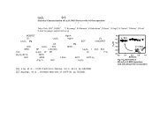
高濃度ボロンドープ試料の 角度分解X線光電子分光による 濃度分布解析
高濃度ボロンドープ試料の 角度分解X線光電子分光による 濃度分布解析
高濃度ボロンドープ試料の 角度分解X線光電子分光による 濃度分布解析

You also want an ePaper? Increase the reach of your titles
YUMPU automatically turns print PDFs into web optimized ePapers that Google loves.
X<br />
<br />
Concentration depth profiling of a heavily-boron-doped Si substrate<br />
**<br />
<br />
*<br />
K. Kakushima, J. Kanehara, K. Tsutsui, T. Hattori, H. Iwai<br />
IGSSE, Tokyo Institute of Technology<br />
*FRC, Tokyo Institute of Technology<br />
1
Lg<br />
Plasma<br />
Doping<br />
SIMS profiles of plasma doped (PD) samples<br />
K. Tsutsui et al., JAP, 104 (2008) 093709.<br />
w/o RTA<br />
Anneal<br />
Diffusion<br />
Xj<br />
after spike-RTA<br />
year 2011 2012 2013 2014 2015<br />
L g<br />
(nm) 24 22 20 18 17<br />
Xj (nm) 10.5 9.5 8.7 8.0 7.3<br />
(ITRS 2010 update, High performance)<br />
+FLA<br />
<br />
2
p + <br />
K. Tsutsui et al., JAP, 104 (2008) 093709.<br />
hν=500eVXXPS<br />
(SPring-8 BL27SU)<br />
B1s<br />
B1s, Si2p 3/2<br />
IMFP1nm<br />
B<br />
<br />
<br />
Si0.5nm<br />
XPSB<br />
30nmSIMS<br />
3
I<br />
⎛ x ⎞<br />
= ∫ ∞ ⎜ − ⎟<br />
0<br />
⎝ λ sinθ<br />
⎠<br />
( z) A c( z + x) σ exp dx<br />
dI<br />
dz<br />
c: σ: <br />
λ: IMFP, A: , θ:<br />
( z) c( z + x)<br />
⎛ x ⎞<br />
= A∫ ∞ σ exp⎜<br />
− ⎟dx<br />
0 dz ⎝ λ sinθ<br />
⎠<br />
z=0<br />
z<br />
(x=0)<br />
<br />
<br />
<br />
x<br />
contribute<br />
for I(z)<br />
c(z)<br />
⎡ = Aσ<br />
⎢ − c ∫ ∞ ⎜ ⎟dx<br />
⎣ λ sinθ<br />
0<br />
⎝ λ sinθ<br />
⎠<br />
A<br />
= −Aσc( z) + I( z)<br />
λ sinθ<br />
<br />
1 dI<br />
( )<br />
( z)<br />
1<br />
1<br />
c z = − + I( z)<br />
c0 Aσ<br />
dz λσ sinθ<br />
=<br />
1<br />
⎛ x ⎞ ⎤<br />
( z) + c( z + x) exp − ⎥ ⎦<br />
I<br />
λσ sinθ<br />
( z)<br />
4
(abruptness)<br />
Undrestimation of surface<br />
concentration, c 0 /c(z)<br />
1.0<br />
0.8<br />
0.6<br />
0.4<br />
0.2<br />
λsinθ=0.5nm<br />
c<br />
c<br />
0<br />
= a a<br />
λsinθ=1.0nm<br />
( z) + ln( 10) λ sinθ<br />
0<br />
0 2 4 6 8 10<br />
Abruptness (a), (nm/decade)<br />
c<br />
B concentration (cm -3 )<br />
( z)<br />
= −<br />
10 22<br />
10 21<br />
10 20<br />
10 19<br />
10 18<br />
10 17<br />
1 dI<br />
Aσ<br />
dz<br />
( z)<br />
1<br />
+ I<br />
λσ sinθ<br />
steep profile at surface<br />
after RTA<br />
before RTA<br />
SIMS<br />
10 16 0 5 10 15 20 25 30 35<br />
Distance from surface (nm)<br />
( z)<br />
<br />
λsinθ<br />
Spike-RTA34nm/dec.<br />
5
1. <br />
<br />
2. SiO 2 <br />
XPS<br />
<br />
B 2 H 6 (He)<br />
(as doped)<br />
spike-RTA:1075 o C<br />
<br />
SPring-8 BL26SU<br />
hν=500eV, B1s, Si2p<br />
TOA=15~80 o<br />
6
O 3 HF<br />
(0.5nm)<br />
XPS<br />
<br />
c<br />
c<br />
0<br />
=<br />
( z)<br />
TOA: θ=80 o<br />
1<br />
I<br />
λσ sinθ<br />
<br />
= −<br />
( z)<br />
1 dI<br />
Aσ<br />
dz<br />
( z)<br />
1<br />
+ I<br />
λσ sinθ<br />
B concentration<br />
( z)<br />
(x10 21 cm -3 )<br />
3.5<br />
3.0<br />
2.5<br />
2.0<br />
1.5<br />
1.0<br />
0.5<br />
0.0<br />
<br />
<br />
0 1 2 3 4 5<br />
Depth (nm)<br />
<br />
Si<br />
7
1. <br />
2. /SiO 2 <br />
D.-A. Luh et al., Phys. Rev. Lett. 79, 3014 (1997).<br />
3. Si2pSi2p 3/2 <br />
G. Hollinger et al., Appl. Phys. Lett., 44, pp. 93-95 (1984).<br />
4. SiO 2 SiBλ1.18, 1.00nm<br />
5. σ(Si2p 3/2 )/σ(B1s)=3.18<br />
SiO 2<br />
T. Hattori, et al., J. Vac. Sci. Technol., B 11, 1528-1532 (1993).<br />
S. Tanuma et al., Surf. Interface Anal., 17, pp. 927-939 (1991).<br />
J. J. Yeh and I. Lindau, At. Data and Nucl. Data Tables 32, 1 (1985).<br />
6. SiO 2 B<br />
<br />
d<br />
Si<br />
φ<br />
θ<br />
I(SiO 2 )<br />
I(Si)<br />
7. z=5~10nm<br />
SIMS<br />
8
B1sSi2p<br />
Intensity (Arb. Units)<br />
Intensity (Arb. Units)<br />
before RTA<br />
BO x<br />
B<br />
TOA=80 o<br />
20 o<br />
205 195 180 175<br />
Binding energy (eV)<br />
after RTA<br />
105<br />
after RTA SiO<br />
BO 2<br />
x<br />
B<br />
15 o<br />
TOA=80 o<br />
205 195 180 175<br />
Binding energy (eV)<br />
Intensity (Arb. Units)<br />
Intensity (Arb. Units)<br />
before RTA<br />
TOA=80 o<br />
SiO 2<br />
20 o<br />
Si<br />
110 100 95<br />
Binding energy (eV)<br />
TOA=80 o<br />
15 o<br />
Si<br />
110 105 100 95<br />
Binding energy (eV)<br />
Si2p<br />
9
Intensity ratio (Arb. Units)<br />
I(Si)<br />
I(SiO)<br />
before RTA<br />
after RTA<br />
0 30 60 90<br />
TOA (degree)<br />
SiO 2<br />
SiO 2<br />
0.87nm<br />
λ Si2p3/2,Si<br />
0.24nm<br />
RTA<br />
1.47nm<br />
(SiSi2pIMFP)<br />
0.43nm<br />
Spike-RTA<br />
SiIMFP<br />
10
Intensity ratio (Arb. Units)<br />
I(BO)<br />
I(SiO)<br />
after RTA<br />
before RTA<br />
0 30 60 90<br />
TOA (degree)<br />
RTA<br />
SiO 2<br />
SiO 2<br />
0.87nm<br />
0.87nm<br />
0.60nm<br />
1.5x10 20 cm -3 <br />
1.5x10 21 cm -3<br />
0.6nm<br />
Si<br />
11
Si<br />
Intensity ratio (Arb. Units)<br />
after RTA<br />
I(B)<br />
I(Si)<br />
before RTA<br />
0 30 60 90<br />
TOA (degree)<br />
B concentration<br />
(x10 21 cm -3 )<br />
3.5<br />
3.0<br />
2.5<br />
2.0<br />
1.5<br />
<br />
1.0<br />
0.5<br />
<br />
0.0<br />
0 1 2 3 4 5<br />
Depth (nm)<br />
c(z)<br />
IMFP<br />
λ B1s,Si<br />
0.35nm<br />
(SiB1sIMFP)<br />
0.61nm<br />
Spike-RTA<br />
SiIMFP<br />
12
Si<br />
B concentration (cm -3 )<br />
(x10 21 )<br />
3<br />
2<br />
1<br />
0<br />
-2<br />
SiO 2<br />
surface<br />
surface<br />
-1<br />
0<br />
Si<br />
4.8x10 13 cm -3<br />
3.8x10 13 cm -3<br />
1 2 3 4<br />
Distance from SiO 2 /Si interface (nm)<br />
<br />
SiO 2 <br />
<br />
13
0.8nm<br />
<br />
XPS<br />
SiO 2 2<br />
<br />
14