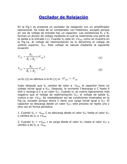
Oscilador de Relajación - Elo.jmc.utfsm.cl
Oscilador de Relajación - Elo.jmc.utfsm.cl
Oscilador de Relajación - Elo.jmc.utfsm.cl

Create successful ePaper yourself
Turn your PDF publications into a flip-book with our unique Google optimized e-Paper software.
<strong>Oscilador</strong> <strong>de</strong> <strong>Relajación</strong><br />
En la Fig.1 se presenta un oscilador <strong>de</strong> relajación con un amplificador<br />
operacional. Se trata <strong>de</strong> un comparador con histéresis, excepto porque<br />
en vez <strong>de</strong> voltaje <strong>de</strong> entrada hay un capacitor. Las resistencias R1 y R2<br />
forman un divisor <strong>de</strong> voltaje mediante el cual se realimenta una parte <strong>de</strong><br />
la salida a la entrada (+). Cuando Vo esta en +Vsat, como se muestra en<br />
la Fig.1a. Al voltaje <strong>de</strong> realimentación se le <strong>de</strong>nomina el voltaje <strong>de</strong><br />
umbral superior, VUT. Este voltaje se calcula mediante la siguiente<br />
ecuación<br />
R2<br />
V UT = ( + Vsat<br />
)<br />
R + R<br />
(1)<br />
1<br />
R2<br />
VLT = ( −V<br />
R + R<br />
1<br />
2<br />
2<br />
sat<br />
)<br />
+ V = −V<br />
La Ec.(2) es idéntica a la Ec.(1) si sat sat<br />
Justo <strong>de</strong>spués que Vo cambia <strong>de</strong> valor a –Vsat, el capacitor tiene un<br />
voltaje inicial igual a VUT. Después, la corriente I - <strong>de</strong>scarga a C hasta 0<br />
Volt y recarga a C a un valor VLT. Cuando VC se vuelve ligeramente más<br />
negativo que el voltaje <strong>de</strong> realimentación VLT, el voltaje <strong>de</strong> salida Vo<br />
vuelve a ser +Vsat. Se reestablecen así las condiciones mostradas en la<br />
Fig.1a, excepto porque ahora C tiene una carga inicial igual a VLT. El<br />
capacitor se <strong>de</strong>scarga <strong>de</strong>s<strong>de</strong> un valor VUT; este proceso se repite una y<br />
otra vez en forma periódica.<br />
1. Cuando Vo = -Vsat, C se <strong>de</strong>scarga <strong>de</strong>s<strong>de</strong> el valor VUT hasta el valor VLT<br />
y cambia <strong>de</strong> Vo a +Vsat.<br />
2. Cuando Vo = +Vsat, c se carga <strong>de</strong>s<strong>de</strong> el valor VLT hasta el valor VUT y<br />
cambio a <strong>de</strong> Vo a –Vsat.<br />
(2)
I + carga a C<br />
hasta V UT<br />
I - carga a C <strong>de</strong>s<strong>de</strong> V UT<br />
hasta V LT<br />
- V C +<br />
C<br />
+ V C -<br />
+<br />
-<br />
+<br />
-<br />
R f<br />
+V<br />
-<br />
+<br />
-V<br />
V UT<br />
R f<br />
+V<br />
-<br />
+<br />
-V<br />
V LT<br />
R 1<br />
R 2<br />
R 1<br />
R 2<br />
V o = +V sat<br />
(a) Cuando V o = +V sat , V C se carga al valor V UT<br />
- V C +<br />
Voltaje inicial = V UT<br />
V o = -V sat<br />
(b) Cuando V o = -V sat , V C se carga al valor V LT<br />
I +<br />
Frecuencia <strong>de</strong> oscilación<br />
I -<br />
Figura 1. Multivibrador<br />
astable (R 1 =100kΩ, R 2 =86kΩ).<br />
En la Fig.2 se aprecian las formas <strong>de</strong> onda <strong>de</strong>l capacitor y <strong>de</strong>l voltaje <strong>de</strong><br />
salida <strong>de</strong>l multivibrador astable.<br />
Para simplificar el cálculo <strong>de</strong>l tiempo <strong>de</strong> carga <strong>de</strong>l capacitor se escoge R2<br />
<strong>de</strong> manera que sea igual a 0.86R1. Los intervalos <strong>de</strong> tiempo t1 y t2<br />
muestran como cambian VC y Vo con el tiempo. Los intervalos <strong>de</strong> tiempo<br />
t1 y t2 son iguales al producto <strong>de</strong> Rf y C<br />
T = 2*Rf*C cuando R2 = 0.86R1 (3)
15<br />
10<br />
V UT<br />
5<br />
0<br />
-5<br />
V LT<br />
-10<br />
-15<br />
V o<br />
V 0 = +V sat<br />
T = 2RC = 1/f<br />
V C<br />
t 1 = R fC t 2 = R fC<br />
V 0 = -V sat<br />
Tiempo<br />
Figura 2. Formas <strong>de</strong> onda <strong>de</strong> voltaje <strong>de</strong>l<br />
multivibrador <strong>de</strong> la Fig.1<br />
Ejemplo: Para la Fig.2<br />
con R1 = 100kΩ R2 = 86kΩ Rf = 100kΩ<br />
C = 0.1µF +Vsat = 15V -Vsat = -15V<br />
Resolución:<br />
V<br />
V<br />
UT<br />
LT<br />
86kΩ<br />
= ( 15)<br />
186kΩ<br />
≈ 7V<br />
86kΩ<br />
= ( −15)<br />
≈ −7V<br />
186kΩ<br />
T = ( 2)(<br />
100kΩ)(<br />
0.<br />
1µ<br />
F)<br />
= 20ms<br />
1 1<br />
f = = = 50Hz<br />
T 20ms<br />
Demostración porque T = 2*Rf*C cuando R2 = 0.86R1.
De la Fig.2 se pue<strong>de</strong>n obtener los valores iniciales y finales <strong>de</strong> carga <strong>de</strong>l<br />
con<strong>de</strong>nsador C<br />
Vi = VLT Vf = +Vsat VC(t1) = VUT<br />
Aplicando:<br />
V<br />
C<br />
= V<br />
f<br />
+ ( V<br />
i<br />
−V<br />
Desarrollando :<br />
f<br />
) e<br />
−t<br />
/ R<br />
f<br />
C<br />
⎛ + Vsat<br />
−V<br />
LT ⎞<br />
t1 = R f C ln⎜<br />
⎟<br />
⎜<br />
⎟<br />
⎝ + Vsat<br />
−V<br />
(4)<br />
LT ⎠<br />
reemplazando (1) y (2) en (4)<br />
= R<br />
t1 f<br />
⎛ R1<br />
+ 2R<br />
C ln<br />
⎜<br />
⎝ R1<br />
con R = 0.86R1<br />
2<br />
⎞<br />
⎟<br />
⎠<br />
⎛ R1<br />
+ 2*<br />
0.<br />
86R1<br />
⎞<br />
t1 = R f C ln<br />
⎜<br />
= R f C ≈ R f C<br />
R ⎟ ln( 2.<br />
72)<br />
⎝ 1 ⎠<br />
como t1 = t2<br />
T = 2*Rf*C (5)
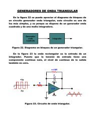
Generador <strong>de</strong> Onda Triangular<br />
En la Fig.6 se muestra un circuito generador <strong>de</strong> onda triangular bipolar<br />
básico. La onda triangular VA, se obtiene a la salida <strong>de</strong>l circuito<br />
integrador 741. A la salida <strong>de</strong>l comparador 301 se presenta una señal <strong>de</strong><br />
onda cuadrada VB.<br />
R i = 14kΩ<br />
+V sat<br />
-V sat<br />
15<br />
C = 0.05µF<br />
pR = 28kΩ<br />
+15V<br />
-<br />
741<br />
R = 10kΩ<br />
+15V<br />
-<br />
+<br />
301<br />
-15V +<br />
-15V<br />
V A<br />
(a) El circuito integrador 741 y el ciecuito comparador 301<br />
se conectan para construir un generador <strong>de</strong> onda triangular<br />
10<br />
5<br />
0<br />
-5<br />
-10<br />
-15<br />
V A y V B (V)<br />
V B en función <strong>de</strong> t<br />
V A en función<br />
<strong>de</strong> t<br />
1 2 3<br />
(b) Formas <strong>de</strong> onda<br />
V UT<br />
t (ms)<br />
Figura 6. El circuito generador <strong>de</strong> onda triangular bipolar<br />
en (a) produce las señales <strong>de</strong> onda cuadrada y<br />
triangular que se muestran en (b). (a) La frecuencia<br />
básica <strong>de</strong>l oscilador generador <strong>de</strong> la onda triangular<br />
a 1kHz; (b) formas <strong>de</strong> onda <strong>de</strong>l voltaje <strong>de</strong> salida.<br />
V LT<br />
V B
Para compren<strong>de</strong>r como funciona el circuito, obsérvese el intervalo<br />
comprendido entre 0 y 1 ms en la Fig.1. Suponga que VB está en el nivel<br />
alto, en el valor +Vsat. En estas condiciones se provoca el flujo <strong>de</strong> una<br />
corriente constante (Vsat / Ri) a través <strong>de</strong>l con<strong>de</strong>nsador C (<strong>de</strong> izquierda a<br />
<strong>de</strong>recha), volviendo VA negativo, que pasa <strong>de</strong> VUT a VLT. Cuando VA llega<br />
a este valor, el pin (+) <strong>de</strong>l 301 se vuelve negativo y VB cambia<br />
súbitamente al valor –Vsat y t = 1ms.<br />
Cuando el valor <strong>de</strong> VB es –Vsat, se produce un flujo <strong>de</strong> corriente<br />
constante (Vsat / Ri) (<strong>de</strong> <strong>de</strong>recha a izquierda) a través <strong>de</strong> C, convirtiendo<br />
a VA en positivo, <strong>de</strong>s<strong>de</strong> el valor VLT hasta VUT (obsérvese lo que suce<strong>de</strong><br />
en el intervalo que va <strong>de</strong> 1 a 2 ms). En cuanto VA alcanza el valor VUT,<br />
cuando t = 2 ms, el pin (+) se vuelve positivo y VB cambia súbitamente<br />
a +Vsat. Lo anterior da lugar al inicio <strong>de</strong>l siguiente ci<strong>cl</strong>o <strong>de</strong> oscilación.<br />
Frecuencia <strong>de</strong> operación<br />
Los valores peca <strong>de</strong> la onda triangular se calculan a partir <strong>de</strong> la relación<br />
que existe entre las resistencias pR y R y los voltajes <strong>de</strong> saturación.<br />
Todos ellos se calculan <strong>de</strong> la siguiente manera<br />
V<br />
V<br />
UT<br />
LT<br />
−Vsat<br />
= −<br />
(6)<br />
p<br />
+ Vsat<br />
= −<br />
(7)<br />
p<br />
en don<strong>de</strong><br />
pR<br />
p = (8)<br />
R<br />
Si los voltajes <strong>de</strong> saturación son razonablemente iguales, la frecuencia<br />
<strong>de</strong> operación estará dada por:<br />
f<br />
p<br />
= (9)<br />
4R<br />
C<br />
i<br />
Ejemplo: El generador <strong>de</strong> la Fig.6 oscila a una frecuencia <strong>de</strong> 1kHz y sus<br />
valores peak reales son aproximadamente ±5V. Calcule los valores<br />
correspondientes <strong>de</strong> pR, Ri y C
Resolución:<br />
Los valores reales <strong>de</strong> +Vsat = +14.2V y el <strong>de</strong> –Vsat = -13V para una<br />
fuente <strong>de</strong> ±15V. Por lo tanto<br />
−V<br />
p = −<br />
V<br />
sat<br />
UT<br />
−13.<br />
8<br />
= − =<br />
5<br />
+ 2.<br />
76<br />
Si R = 10kΩ y pR = 28kΩ<br />
≈<br />
2.<br />
8<br />
Luego se elige el valor <strong>de</strong> Ri y C. primero se elige un valor tentativo para<br />
C = 0.05µF. luego se calcula el valor <strong>de</strong> Ri, y se observa si Ri resulta<br />
mayor a 10kΩ. De la ecuación (4)<br />
R i<br />
p 2.<br />
8<br />
= =<br />
= 14kΩ<br />
4 fC 4*<br />
1000*<br />
0.<br />
05µ<br />
En la práctica seria recomendable construir Ri con una resistencia <strong>de</strong><br />
12kΩ en serie con un potenciómetro <strong>de</strong> 0 a 5kΩ. Este se ajusta para una<br />
frecuencia <strong>de</strong> oscilación precisa <strong>de</strong> 1kHz.
Generador unipolar <strong>de</strong> onda triangular<br />
El circuito <strong>de</strong>l generador unipolar <strong>de</strong> onda triangular <strong>de</strong> la Fig.2 se pue<strong>de</strong><br />
modificar <strong>de</strong> manera que produzca una onda triangular unipolar. Basta<br />
con conectar un diodo en serie con pR como se precisa en la Fig.2.<br />
Cuando el valor <strong>de</strong> VB es Vsat, el diodo interrumpe el flujo <strong>de</strong> la corriente<br />
a través <strong>de</strong> pR y <strong>de</strong>fine VLT a 0V. Cuando VB es –Vsat, el diodo permite el<br />
flujo <strong>de</strong> corriente por pR y <strong>de</strong>fine el valor <strong>de</strong> VLT como:<br />
V<br />
UT<br />
−Vsat<br />
+ 0.<br />
6<br />
= (10)<br />
p<br />
R i = 14kΩ<br />
+V sat<br />
-V sat<br />
15<br />
10<br />
5<br />
0<br />
-5<br />
-10<br />
-15<br />
C = 0.05µF<br />
+15V<br />
-<br />
741<br />
R = 10kΩ<br />
+15V<br />
-<br />
+<br />
301<br />
-15V +<br />
-15V<br />
V A<br />
pR = 28kΩ<br />
(a) Generador <strong>de</strong> onda triangular unipolar.<br />
V A y V B (V)<br />
V B en función <strong>de</strong> t<br />
V A en función<br />
<strong>de</strong> t<br />
1 2 3<br />
(b) Formas <strong>de</strong> onda<br />
V UT<br />
t (ms)<br />
Figura 7. El diodo D en (a) convierte el<br />
generador <strong>de</strong> onda triangular bipolar en<br />
un generador <strong>de</strong> onda triangular unipolar.<br />
Las formas <strong>de</strong> onda correspondientes<br />
se muestran en (b).<br />
D<br />
V B
La frecuencia <strong>de</strong> oscilación se calcula aproximadamente por:<br />
f<br />
p<br />
≈ (11)<br />
2R<br />
C<br />
Ejemplo:<br />
i<br />
Calcule el voltaje peak aproximado y la frecuencia <strong>de</strong>l generador <strong>de</strong><br />
onda triangular <strong>de</strong> la Fig.7<br />
Resolución:<br />
pR 28kΩ<br />
p = = = 2.<br />
8<br />
R 10kΩ<br />
De la Ec.(10)<br />
V<br />
UT<br />
−V<br />
=<br />
sat<br />
p<br />
+<br />
0.<br />
6<br />
De la Ec.(11)<br />
( −13.<br />
8 +<br />
=<br />
2.<br />
8<br />
0.<br />
6)<br />
≈ 4.<br />
7V<br />
p<br />
2.<br />
8<br />
f = =<br />
= 1000Hz<br />
2R<br />
C 2(<br />
28kΩ)(<br />
0.<br />
05µ<br />
F)<br />
i
Generador <strong>de</strong> onda diente <strong>de</strong> sierra<br />
Funcionamiento <strong>de</strong>l circuito:<br />
En la Fig.8 se muestra el circuito <strong>de</strong> un generador <strong>de</strong> onda <strong>de</strong> diente <strong>de</strong><br />
sierra. Dado que Ei es negativo, la única opción <strong>de</strong> Vo ramp es aumentar.<br />
La tasa <strong>de</strong> aumento <strong>de</strong>l voltaje <strong>de</strong> rampa es constante en las siguientes<br />
condiciones<br />
V<br />
o ramp =<br />
t<br />
Ei<br />
R C<br />
Tensión en C<br />
i<br />
(12)<br />
I<br />
VC = t<br />
(13)<br />
C<br />
Velocidad <strong>de</strong> barrido =<br />
dV I<br />
= (14)<br />
dt C<br />
El voltaje <strong>de</strong> rampa se monitorea a través <strong>de</strong> la entrada <strong>de</strong>l comparador<br />
301B. Si el valor <strong>de</strong> Vo ramp está por <strong>de</strong>bajo <strong>de</strong>l Vref, la salida en el<br />
comparador es negativa. Los diodos protegen a los transistores <strong>de</strong> una<br />
polarización inversa excesiva.<br />
Cuando Vo ramp aumenta precisamente por encima <strong>de</strong> Vref, la salida <strong>de</strong> Vo<br />
ramp alcanza la saturación positiva. Estas polarizaciones directas<br />
provocan la saturación <strong>de</strong>l transistor QD. Éste se comporta como un<br />
cortocircuito a través <strong>de</strong>l capacitor integrador C. Éste se <strong>de</strong>scarga<br />
rápidamente a través <strong>de</strong> QD hasta un valor <strong>de</strong> 0V. Cuando Vo ramp se<br />
vuelve positivo, activa a<strong>de</strong>más a Q1 y éste cortocircuita al potenciómetro<br />
<strong>de</strong> 10kΩ. Esto provoca que Vref <strong>de</strong>scienda a un valor <strong>de</strong> casi cero Volt.<br />
Conforme C se va <strong>de</strong>scargando hasta llegar a cero Volt, activa<br />
rápidamente a Vo ramp hasta que llega a cero Volt. Vo ramp <strong>de</strong>scien<strong>de</strong> por<br />
<strong>de</strong>bajo <strong>de</strong>l valor <strong>de</strong> Vref, lo que provoca que Vo ramp se vuelva negativo y<br />
<strong>de</strong>sactive a QD. C comienza a <strong>de</strong>scargarse en forma lineal y se inicia la<br />
generación <strong>de</strong> una nueva onda diente <strong>de</strong> sierra.
E i = -1V<br />
15<br />
10<br />
5<br />
0<br />
-5<br />
-10<br />
-15<br />
QD = 2N3904 ó<br />
2N2222<br />
R i = 10kΩ<br />
V o comp y V o ramp (V)<br />
V ref<br />
V o comp<br />
Q D<br />
C = 0.1µF<br />
+15V<br />
-<br />
741<br />
+<br />
-15V<br />
R B = 10kΩ<br />
V o ramp<br />
D<br />
-15V<br />
-<br />
301<br />
+<br />
+15V<br />
5kΩ<br />
0-10kΩ<br />
V ref = 10V<br />
(a) Circuito generador <strong>de</strong> onda diente <strong>de</strong> sierra.<br />
V o comp<br />
10 20<br />
V o ramp<br />
t (ms)<br />
V ref = 10<br />
(b) Salida <strong>de</strong> onda diente <strong>de</strong> sierra<br />
V o ramp y salida <strong>de</strong>l comparador.<br />
5<br />
0<br />
V o ramp (V)<br />
V o comp<br />
10kΩ<br />
Q 1<br />
La rampa se eleva hasta alcanzar<br />
el voltaje pico <strong>de</strong>finido por V ref<br />
5<br />
10<br />
t (ms)<br />
D<br />
La tasa <strong>de</strong> la subida está <strong>de</strong>finida por:<br />
E i /R iC = V o ramp/t<br />
Figura 8. El circuito generador <strong>de</strong> onda diente <strong>de</strong> sierra<br />
<strong>de</strong> (a) tiene las formas <strong>de</strong> onda mostradas en (b) y<br />
(c). La frecuencia <strong>de</strong> oscilación es <strong>de</strong> 100 Hz,<br />
o f=(1/R i C)(E i /V ref ).
Análisis <strong>de</strong> la forma <strong>de</strong> la onda diente <strong>de</strong> sierra:<br />
En la Fig.8b, el voltaje <strong>de</strong> rampa se eleva a una velocidad <strong>de</strong> 1V por<br />
milisegundo, mientras que Vo comp es negativo. A continuación la rampa<br />
cruza el valor Vref, Vo comp se vuelve súbitamente positivo para llevar<br />
rápidamente el voltaje <strong>de</strong> rampa hacia cero Volt. Conforme Vo ramp<br />
cambia rápidamente a 0 V, la salida <strong>de</strong>l comparador cambia al valor <strong>de</strong><br />
saturación negativo. En la Fig.8c se resume el funcionamiento <strong>de</strong> la<br />
rampa.<br />
Procedimiento <strong>de</strong> diseño:<br />
El tiempo correspondiente al periodo <strong>de</strong> una onda diente <strong>de</strong> sierra esta<br />
<strong>de</strong>terminado por<br />
dis tan cia(<br />
subida)<br />
Tiempo ( subida)<br />
= (15)<br />
velocidad ( subida)<br />
<strong>de</strong> (14) con t = T porque t2 es <strong>de</strong>spreciable<br />
T<br />
V<br />
ref<br />
=<br />
Ei<br />
/ RiC<br />
(16)<br />
por lo tanto<br />
⎛ 1 ⎞ Ei<br />
f = ⎜ ⎟<br />
⎜ RiC<br />
⎟<br />
⎝ ⎠ V<br />
ref<br />
Ejemplo <strong>de</strong> diseño :<br />
(17)<br />
Diseñe un generador <strong>de</strong> onda diente <strong>de</strong> sierra que tenga una salida <strong>de</strong><br />
10V <strong>de</strong> peca y una frecuencia <strong>de</strong> 100Hz. Suponga que Ei = 1V y que Vo<br />
tiene que alcanzar una valor <strong>de</strong> 10V en amps (paso 2).<br />
Procedimiento <strong>de</strong> diseño:<br />
1. Diseñe un divisor <strong>de</strong> voltaje mediante el cual se obtenga un voltaje<br />
<strong>de</strong> referencia Vref = +10V en el caso <strong>de</strong>l comparador.
2. Escoja una tasa <strong>de</strong> subida (velocidad <strong>de</strong> barrido) <strong>de</strong> la rampa <strong>de</strong><br />
1V/mseg. Elija una combinación <strong>de</strong> RiC que <strong>de</strong> un valor <strong>de</strong> 1mseg. De<br />
esta manera se elige Ri = 10kΩ y C = 0.1µF [Ec.(8)].<br />
3. Ei <strong>de</strong>be provenir <strong>de</strong> un divisor <strong>de</strong> voltaje y un seguidor <strong>de</strong> voltaje para<br />
<strong>de</strong> esta manera obtener una fuente <strong>de</strong> voltaje i<strong>de</strong>al.<br />
4. El circuito es el mostrado en la Fig.8.<br />
5. Otra opción es elegir un valor tentativo <strong>de</strong> RiC y resolver la Ec.(9)<br />
para Ei.<br />
6. Compruebe los valores <strong>de</strong> diseño en la Ec.(10)<br />
1 ⎛ 1V<br />
⎞<br />
f =<br />
⎜ ⎟ = 100Hz<br />
( 10kΩ)(<br />
0.<br />
1µ<br />
F)<br />
⎝10V<br />
⎠<br />
¿Cómo construir un conversor frecuencia/voltaje?<br />
Al circuito anterior varia Ei en f(t).
Transistor monounión programable<br />
El transistor monounión programable (PUT) es un pequeño tiristor que<br />
aparece en la Fig.9. un PUT se pue<strong>de</strong> utilizar como un oscilador <strong>de</strong><br />
relajación, tal como se muestra en la Fig.9b. el voltaje <strong>de</strong> compuerta VG<br />
se mantiene <strong>de</strong>s<strong>de</strong> la alimentación mediante el divisor resistivo <strong>de</strong>l<br />
voltaje R1 y R2, y <strong>de</strong>termina el voltaje <strong>de</strong> punto <strong>de</strong> pico Vp. en el caso<br />
<strong>de</strong>l UJT, Vp esta fijo para un dispositivo por el voltaje <strong>de</strong> alimentación <strong>de</strong><br />
cd, pero el PUT pue<strong>de</strong> variar al modificar el valor <strong>de</strong>l divisor resistivo R1<br />
y R2. si el voltaje <strong>de</strong>l ánodo VA es menor que el voltaje <strong>de</strong> compuerta VG,<br />
el dispositivo se conservara en su estado inactivo, pero si el voltaje <strong>de</strong><br />
ánodo exce<strong>de</strong> al <strong>de</strong> compuerta en una caída <strong>de</strong> voltaje <strong>de</strong> diodo VD, se<br />
alcanzara el punto <strong>de</strong> pico y el dispositivo se activará. La corriente <strong>de</strong><br />
pico Ip y la corriente <strong>de</strong>l punto <strong>de</strong> valle IV <strong>de</strong>pen<strong>de</strong>n <strong>de</strong> la impedancia<br />
equivalente en la compuerta RG = R1R2/(R1+R2) y <strong>de</strong>l voltaje <strong>de</strong><br />
alimentación <strong>de</strong> cd Vs. en general Rk esta limitado a un valor por <strong>de</strong>bajo<br />
<strong>de</strong> 100Ω.<br />
R y C controlan la frecuencia junto con R1 y R2. el periodo <strong>de</strong> oscilación<br />
T esta dado en forma aproximada por:<br />
T<br />
=<br />
1<br />
f<br />
=<br />
RC lnV<br />
V<br />
Ánodo<br />
Cátodo<br />
s<br />
−V<br />
p<br />
s<br />
Compuerta<br />
⎛ R<br />
= RC ln<br />
⎜<br />
⎜1+<br />
⎝ R<br />
Ánodo<br />
PUT PUT<br />
+<br />
VA C<br />
-<br />
2<br />
1<br />
⎞<br />
⎟<br />
⎠<br />
R<br />
R S<br />
Cátodo<br />
+<br />
V RS<br />
-<br />
(a) Símbolo. (b) Circuito.<br />
Figura 9. Circuito <strong>de</strong> disparo para un PUT.<br />
V S<br />
R 1<br />
Compuerta<br />
R 2<br />
+<br />
V G<br />
-
+<br />
V AK<br />
-<br />
Ánodo<br />
P<br />
N<br />
P<br />
N<br />
+<br />
K<br />
Cátodo<br />
V AG<br />
-<br />
G<br />
Compuerta<br />
Estado<br />
Apagado<br />
V P<br />
V F<br />
V v<br />
V AK<br />
I P I V I F<br />
(a) Circuito equivalente. (b) Curva <strong>de</strong> respuesta <strong>de</strong>l circuito [Fig.9(b)].<br />
don<strong>de</strong> η<br />
=<br />
R<br />
B1<br />
+<br />
V AK<br />
R<br />
-<br />
B1<br />
+ R<br />
Figura 10. Especificaciones <strong>de</strong>l PUT.<br />
B2<br />
A<br />
K<br />
PUT<br />
G<br />
+<br />
V G<br />
-<br />
R B2<br />
R B1<br />
Figura 11. Polarización <strong>de</strong>l PUT.<br />
Región inestable<br />
(-R)<br />
V BB<br />
Estado<br />
Encendido<br />
I A
El potencial <strong>de</strong> disparo (Vp) o voltaje necesario para “disparar” el<br />
dispositivo está dado por Vp = ηVBB + VD.<br />
Sin embargo Vp representa la caída <strong>de</strong> voltaje VAK (la caída <strong>de</strong> voltaje a<br />
través <strong>de</strong>l diodo conductor). Para el silicio, es típicamente 0.7, por lo<br />
tanto Vp = ηVBB + 0.7 = VG + 0.7V<br />
VBB<br />
T = RC ln<br />
V −V<br />
BB<br />
P<br />
o cuando Vp = ηVBB<br />
⎛ R<br />
T = RC ln<br />
⎜<br />
⎜1+<br />
⎝ R<br />
V C<br />
R<br />
C<br />
IpR = VBB - Vp<br />
R<br />
MAX<br />
V<br />
=<br />
BB<br />
I<br />
B1<br />
B2<br />
I A<br />
⎞<br />
⎟<br />
⎠<br />
K<br />
R K<br />
(a) Circuito.<br />
−V<br />
p<br />
p<br />
R B2<br />
R B1<br />
V BB<br />
V BB<br />
V p<br />
V C<br />
Figura 12. Curva <strong>de</strong> respuesta <strong>de</strong>l PUT.<br />
(b) Voltaje <strong>de</strong> disparo <strong>de</strong>l PUT.
R<br />
MIN<br />
V<br />
=<br />
BB<br />
I<br />
−V<br />
V<br />
V C<br />
V K<br />
V G<br />
V<br />
V C<br />
V K =V A -V V<br />
V G =ηV BB<br />
RMIN < R < RMAX<br />
Figura 13. Curvas <strong>de</strong> salida <strong>de</strong> los voltajes <strong>de</strong>l PUT.