Amplificatori Operazionali - Dipartimento di Elettronica ed ...
Amplificatori Operazionali - Dipartimento di Elettronica ed ...
Amplificatori Operazionali - Dipartimento di Elettronica ed ...

Create successful ePaper yourself
Turn your PDF publications into a flip-book with our unique Google optimized e-Paper software.
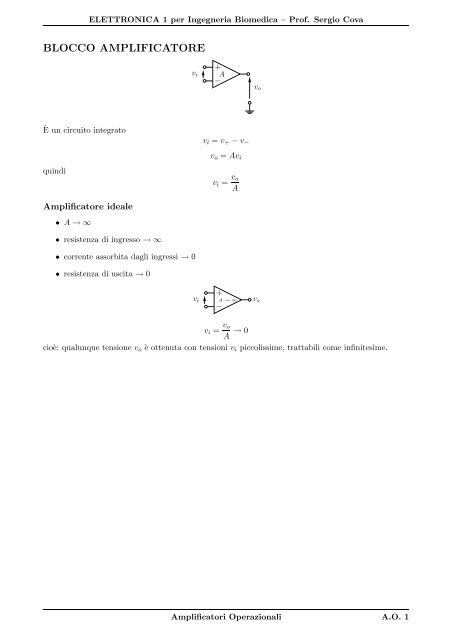
ELETTRONICA 1 per Ingegneria Biome<strong>di</strong>ca – Prof. Sergio Cova<br />
BLOCCO AMPLIFICATORE<br />
È un circuito integrato<br />
quin<strong>di</strong><br />
Amplificatore ideale<br />
• A → ∞<br />
• resistenza <strong>di</strong> ingresso → ∞<br />
• corrente assorbita dagli ingressi → 0<br />
• resistenza <strong>di</strong> uscita → 0<br />
+<br />
vi A<br />
vi<br />
−<br />
vi = v+ − v−<br />
vo = Avi<br />
vi = vo<br />
A<br />
+<br />
A → ∞<br />
−<br />
vi = vo<br />
cioè: qualunque tensione vo è ottenuta con tensioni vi piccolissime, trattabili come infinitesime.<br />
A<br />
→ 0<br />
vo<br />
vo<br />
<strong>Amplificatori</strong> <strong>Operazionali</strong> A.O. 1
ELETTRONICA 1 per Ingegneria Biome<strong>di</strong>ca – Prof. Sergio Cova<br />
CONFIGURAZIONI CIRCUITALI DI BASE<br />
Amplificatore invertente (visto con amplificatore ideale)<br />
Fondamenti:<br />
a) amplificazione A → ∞<br />
b) correnti <strong>di</strong> ingresso amplificatore = 0<br />
da cui si ricava<br />
a)<br />
b)<br />
cioè<br />
vs<br />
+<br />
R1<br />
i1<br />
vi = v+ − v− = 0<br />
i2<br />
R2<br />
−<br />
A<br />
+<br />
<br />
v− = v+ = 0<br />
vi = lim<br />
A→∞<br />
vo<br />
<br />
vo<br />
A<br />
Il terminale negativo dell’amplificatore è una massa (o terra) virtuale.<br />
vs − v−<br />
R1<br />
vs<br />
R1<br />
i1 = i2<br />
= v− − vo<br />
R2<br />
= − vo<br />
R2<br />
Quin<strong>di</strong> il guadagno ideale della configurazione invertente è<br />
Si v<strong>ed</strong>e <strong>di</strong>rettamente:<br />
Gid = vo<br />
vs<br />
= − R2<br />
R1<br />
1. Il morsetto negativo è una massa virtuale: v− = 0<br />
2. nella resistenza R1 scorre i1 = vs<br />
, <strong>di</strong>retta verso l’ingresso dell’amplificatore<br />
R1<br />
3. la corrente i1 prosegue come i2 = i1 nella resisteza R2<br />
4. la tensione ai capi <strong>di</strong> R2 vale i2R2 = vs R2<br />
R1<br />
5. l’uscita dell’amplificatore è più bassa del morsetto <strong>di</strong> ingresso invertente proprio a causa della<br />
caduta <strong>di</strong> tensione su R2<br />
Si trova quin<strong>di</strong><br />
R2<br />
vo = −vs<br />
R1<br />
A.O. 2 <strong>Amplificatori</strong> <strong>Operazionali</strong>
ELETTRONICA 1 per Ingegneria Biome<strong>di</strong>ca – Prof. Sergio Cova<br />
Amplificatore NON invertente (visto con amplificatore ideale)<br />
Fondamenti:<br />
a) amplificazione A → ∞<br />
b) correnti <strong>di</strong> ingresso amplificatore = 0<br />
da cui si ricava<br />
a)<br />
b)<br />
R1<br />
+<br />
vs<br />
i1<br />
i2<br />
R2<br />
−<br />
A<br />
+<br />
vi = v+ − v− = 0<br />
v− = v+ = vs<br />
cioè il terminale negativo dell’amplificatore segue la tensione applicata al terminale positivo<br />
0 − v−<br />
R1<br />
− vs<br />
R1<br />
i1 = i2<br />
= v− − vo<br />
R2<br />
= vs − vo<br />
R2<br />
Quin<strong>di</strong> il guadagno ideale della configurazione invertente è<br />
Si v<strong>ed</strong>e <strong>di</strong>rettamente:<br />
1. il morsetto positivo è a tensione vs<br />
Gid = vo<br />
vs<br />
2. il morsetto negativo è alla stessa tensione<br />
= 1 + R2<br />
R1<br />
3. nella resistenza R1 scorre i1 = − vs<br />
, cioè la corrente è <strong>di</strong>retta dall’ingresso dell’amplificatore<br />
R1<br />
verso massa<br />
4. nella resistenza R2 scorre i2 = i1, cioè <strong>di</strong> uguale valore e <strong>di</strong>retta dall’uscita dell’amplificatore<br />
verso l’ingresso<br />
5. l’uscita dell’amplificatore si trova rispetto a massa più in alto <strong>di</strong> una quantità data dalla somma<br />
delle cadute su R1 <strong>ed</strong> R2<br />
Si trova quin<strong>di</strong><br />
R2<br />
vo = vs + vs<br />
R1<br />
= vs<br />
<br />
1 + R2<br />
<br />
R1<br />
vo<br />
<strong>Amplificatori</strong> <strong>Operazionali</strong> A.O. 3
ELETTRONICA 1 per Ingegneria Biome<strong>di</strong>ca – Prof. Sergio Cova<br />
Amplificatore invertente (visto con guadagno A finito)<br />
Fondamenti:<br />
vs<br />
a) amplificazione molto grande A ≫ 1<br />
b) correnti <strong>di</strong> ingresso amplificatore trascurabili ≃ 0<br />
da cui segue<br />
a)<br />
b)<br />
+<br />
R1<br />
i1<br />
i2<br />
R2<br />
−<br />
A<br />
+<br />
vi = v+ − v− = vo<br />
A<br />
1<br />
R1<br />
vo<br />
vs − v−<br />
R1<br />
<br />
vs + vo<br />
<br />
A<br />
v− = − vo<br />
A<br />
i1 = i2<br />
<br />
1 + 1 1<br />
+<br />
A A<br />
= v− − vo<br />
R2<br />
= 1<br />
Quin<strong>di</strong> il guadagno reale della configurazione invertente è<br />
cioè<br />
G = vo<br />
vs<br />
G = Gid<br />
= − R2<br />
R1<br />
R2<br />
R2<br />
R1<br />
<br />
− vo<br />
<br />
(piccola)<br />
− vo<br />
A<br />
= − R2<br />
vs<br />
R1<br />
1<br />
1 + 1+ R 2<br />
R1<br />
A<br />
1<br />
1 + 1+ R 2<br />
R1<br />
A<br />
infatti G → Gid per A → ∞.<br />
Il guadagno d’anello nella configurazione controreazionata è:<br />
Perciò<br />
che, per GL → ∞ si riduce a G = Gid<br />
GL = −A R1<br />
R1 + R2<br />
1<br />
G = Gid<br />
1 − 1<br />
GL<br />
= − A<br />
1 + R2<br />
R1<br />
A.O. 4 <strong>Amplificatori</strong> <strong>Operazionali</strong><br />
vo
ELETTRONICA 1 per Ingegneria Biome<strong>di</strong>ca – Prof. Sergio Cova<br />
Amplificatore NON invertente (visto con guadagno A finito)<br />
Fondamenti:<br />
a) amplificazione molto grande A ≫ 1<br />
R1<br />
+<br />
b) correnti <strong>di</strong> ingresso amplificatore trascurabili ≃ 0<br />
da cui segue<br />
a)<br />
b)<br />
infine:<br />
cioè<br />
vo<br />
vs<br />
i1<br />
i2<br />
R2<br />
−<br />
A<br />
+<br />
vi = v+ − v− = vo<br />
A<br />
G = vo<br />
vs<br />
vo<br />
(piccola)<br />
v− = v+ − vo<br />
A = vs − vo<br />
A<br />
vo<br />
R2<br />
vo =<br />
<br />
1 + 1<br />
A<br />
=<br />
0 − v−<br />
R1<br />
= v−<br />
i1 = i2<br />
= v− − vo<br />
R2<br />
1<br />
R1<br />
+ 1<br />
<br />
R2<br />
R1 + R2<br />
vo = v−<br />
R1<br />
<br />
vs − vo<br />
R1 + R2<br />
R1<br />
A<br />
<br />
<br />
1 + R2<br />
<br />
R1<br />
G = Gid<br />
R1 + R2<br />
1<br />
R1<br />
1 + 1 R1+R2<br />
A R1<br />
1<br />
G = Gid<br />
1 − 1<br />
GL<br />
R1 + R2<br />
= vs<br />
R1<br />
1<br />
1 + 1 R1+R2<br />
A R1<br />
<strong>Amplificatori</strong> <strong>Operazionali</strong> A.O. 5
ELETTRONICA 1 per Ingegneria Biome<strong>di</strong>ca – Prof. Sergio Cova<br />
Guadagno dell’anello <strong>di</strong> controreazione<br />
R1<br />
R2<br />
−<br />
+ A<br />
Consideriamo il guadagno A finito, e percorriamo l’anello:<br />
1. dall’ingresso invertente all’uscita passando dall’amplificatore<br />
2. dall’uscita all’ingresso invertente passando dalla rete <strong>di</strong> reazione<br />
si trova quin<strong>di</strong><br />
1. il segnale <strong>di</strong> prova viene trasferito dall’ingresso invertente all’uscita con funzione <strong>di</strong> trasferimento<br />
(amplificatore)<br />
−A<br />
2. il segnale <strong>di</strong> uscita viene trasferito all’ingresso invertente con funzione <strong>di</strong> trasferimento (partizione<br />
resistiva)<br />
R1<br />
R1 + R2<br />
Il guadagno d’anello si ottiene moltiplicando le due funzioni <strong>di</strong> trasferimento trovate<br />
GL = −A R1<br />
R1 + R2<br />
N.B. 1 L’anello <strong>di</strong> reazione è uguale per entrambe le configurazioni viste (invertente e non invertente)<br />
N.B. 2 Si chiama CONTROreazione perché il segnale riportato al morsetto <strong>di</strong> ingresso si oppone al<br />
segnale iniettato<br />
A.O. 6 <strong>Amplificatori</strong> <strong>Operazionali</strong>
ELETTRONICA 1 per Ingegneria Biome<strong>di</strong>ca – Prof. Sergio Cova<br />
Effetto del guadagno finito in sistemi controreazionati<br />
Consideriamo un sistema controreazionato, con A e B funzioni <strong>di</strong> trasferimento<br />
Il guadagno d’anello è<br />
mentre il guadagno reale è<br />
vs<br />
+<br />
+ A vo<br />
−<br />
B<br />
GL = −AB<br />
G = vo<br />
vs<br />
Per A → ∞ si trova G → 1<br />
B = Gid (caso ideale)<br />
Nel caso reale<br />
G = 1<br />
B<br />
1<br />
1 + 1<br />
AB<br />
=<br />
= Gid<br />
A<br />
1 + AB<br />
1<br />
1 + 1<br />
AB<br />
1<br />
= Gid<br />
1 − 1<br />
GL<br />
Si può partire da qui e ritrovare quanto già visto per gli amplificatori operazionali.<br />
Applicazione al caso della configurazione NON invertente<br />
R1<br />
+<br />
vs<br />
R2<br />
−<br />
A<br />
+<br />
Partendo dal risultato ottenuto per i sistemi controreazionati e ponendo<br />
A = A<br />
(cioè il guadagno del blocco <strong>di</strong> andata è uguale al guadagno dell’operazionale)<br />
si ottiene<br />
vo<br />
vs<br />
= 1<br />
B<br />
1<br />
1 + 1<br />
AB<br />
B =<br />
=<br />
R1<br />
R1 + R2<br />
<br />
1 + R2<br />
<br />
R1<br />
Applicazione al caso della configurazione invertente<br />
vs<br />
+<br />
R1<br />
R2<br />
−<br />
A<br />
+<br />
1<br />
vo<br />
1 + 1 R1+R2<br />
A R1<br />
In questo caso l’anello <strong>di</strong> reazione è lo stesso, ma il segnale vs non è applicato <strong>di</strong>rettamente al morsetto<br />
dell’amplificatore. Lo schema equivalente in questo caso è<br />
vo<br />
<strong>Amplificatori</strong> <strong>Operazionali</strong> A.O. 7
da cui si ricava<br />
Sostituendo<br />
si trova<br />
ELETTRONICA 1 per Ingegneria Biome<strong>di</strong>ca – Prof. Sergio Cova<br />
vo<br />
vs<br />
= −C 1<br />
B<br />
vs<br />
1<br />
1 + 1<br />
AB<br />
+<br />
+ C<br />
−A vo<br />
vo<br />
vs<br />
+<br />
= −AC<br />
1 + AB<br />
B =<br />
C =<br />
B<br />
= −C 1<br />
B<br />
A = A<br />
R1<br />
R1 + R2<br />
R2<br />
R1 + R2<br />
= − R2 R1 + R2<br />
R1 + R2 R1<br />
1<br />
1 + 1<br />
AB<br />
1<br />
1 + 1 R1+R2<br />
A R1<br />
A.O. 8 <strong>Amplificatori</strong> <strong>Operazionali</strong><br />
= − R2<br />
R1<br />
1<br />
1 + 1 R1+R2<br />
A R1
ELETTRONICA 1 per Ingegneria Biome<strong>di</strong>ca – Prof. Sergio Cova<br />
Blocco amplificatore con guadagno finito e banda finita<br />
Consideriamo anche la banda limitata da un singolo polo a ω = ωp. Quin<strong>di</strong> la funzione <strong>di</strong> trasferimento<br />
dell’amplificatore è<br />
A = A0<br />
→<br />
1 + sτp<br />
A0<br />
=<br />
1 + jωτp<br />
A0<br />
1 + j ω<br />
ωp<br />
dove ωp = 1<br />
τp .<br />
Diagramma <strong>di</strong> Bode <strong>di</strong> |A|<br />
log |A|<br />
Asintoti:<br />
A0<br />
a) a bassa frequenza, per ω ≪ ωp, l’asintoto è |A| = A0<br />
b) ad alta frequenza, per ω ≫ ωp, l’asintoto è |A| = A0<br />
ω<br />
ωp<br />
|A| = ωT<br />
ω<br />
ωp<br />
|A| = A0<br />
ωτp<br />
|A| = A0<br />
ωT<br />
ω<br />
= A0ωp<br />
ω ; definendo ωT = A0ωp si trova<br />
dove ωT è la pulsazione alla quale si ha |A| = 1. Si v<strong>ed</strong>e che alle alte frequenze il prodotto |A| ω = ωT<br />
è costante; essendo il prodotto tra il guadagno |A| e la banda ω, viene chiamato prodotto guadagno–<br />
banda, ovvero Gain–BandWidth Product (GBWP).<br />
<strong>Amplificatori</strong> <strong>Operazionali</strong> A.O. 9
ELETTRONICA 1 per Ingegneria Biome<strong>di</strong>ca – Prof. Sergio Cova<br />
Effetto della banda finita (singolo polo) dell’amplificatore in un sistema controreazionato<br />
con rete resistiva<br />
Il guadagno vale<br />
vs<br />
+<br />
+ A vo<br />
−<br />
G = vo<br />
vs<br />
Consideriamo che il sistema sia composto da:<br />
=<br />
B<br />
A<br />
1 + AB<br />
• amplificatore con banda limitata da un polo semplice<br />
A = A0<br />
1 + j ω<br />
ωp<br />
• rete <strong>di</strong> reazione (e quin<strong>di</strong> B) in<strong>di</strong>pendente da ω (contenente solo resistenze)<br />
Quin<strong>di</strong> il guadagno vale<br />
In<strong>di</strong>cando con<br />
e<br />
si trova<br />
Asintoti:<br />
G(ω) =<br />
=<br />
=<br />
=<br />
G0 =<br />
ωpR<br />
A0<br />
1+j ω<br />
ωp<br />
1 + B A0<br />
1+j ω<br />
ωp<br />
A0<br />
1 + A0B<br />
A0<br />
1 + A0B<br />
A0<br />
1 + A0B<br />
=<br />
1<br />
1 + j ω<br />
ωp<br />
1<br />
1 + j ω<br />
A0ωp<br />
1<br />
1 + j ω<br />
ωT<br />
1<br />
1+A0B<br />
A0<br />
1+A0B<br />
A0<br />
1+A0B<br />
A0<br />
1 + A0B −−−−−→<br />
A0B→∞<br />
= ωT<br />
G0<br />
1<br />
B<br />
1 + A0B<br />
= ωT<br />
A0<br />
ωpR = ωP (1 + A0B) = ωP (1 + GL) ≃ ωPGL<br />
G(ω) = G0<br />
1<br />
1 + j ω<br />
ω T<br />
G0<br />
a) a bassa frequenza, per ω ≪ ωpR , l’asintoto è G(ω) = G0<br />
=<br />
=<br />
1<br />
= G0<br />
1 + j ω<br />
ωpR ωpR b) ad alta frequenza, per ω ≫ ωpR , l’asintoto è G(ω) = G0 ω = ✚ G0 ωT 1 ωT<br />
ω = ω ✚✚G0<br />
Notare che l’asintoto ad alta frequenza è lo stesso<br />
• per l’amplificatore A non controreazionato<br />
• per l’amplificatore controreazionato con resistenze<br />
A.O. 10 <strong>Amplificatori</strong> <strong>Operazionali</strong>
La controreazione<br />
ELETTRONICA 1 per Ingegneria Biome<strong>di</strong>ca – Prof. Sergio Cova<br />
log |A|<br />
A0<br />
Amplificatore non reazionato<br />
Amplificatore reazionato<br />
ωp ωpR ωT<br />
G0 = A0<br />
1+A0B<br />
a) riduce il guadagno in continua del fattore 1 + A0B = 1 − GL ≃ −GL = A0B<br />
b) innalza il limite <strong>di</strong> banda da ωp a ωpR dello stesso fattore 1 + A0B = 1 − GL ≃ −GL = A0B<br />
f<br />
≃ 1<br />
B<br />
<strong>Amplificatori</strong> <strong>Operazionali</strong> A.O. 11
ELETTRONICA 1 per Ingegneria Biome<strong>di</strong>ca – Prof. Sergio Cova<br />
Amplificatore NON invertente<br />
Il risultato ottenuto per sistemi controreazionati si applica <strong>di</strong>rrettamente alla configurazione non<br />
invertente<br />
Amplificatore invertente<br />
con C = R2<br />
R1+R2<br />
si ha<br />
vs<br />
e B = R1<br />
R1+R2 .<br />
vs<br />
+<br />
R1<br />
+<br />
R2<br />
−<br />
A<br />
+<br />
+ C<br />
−A vo<br />
F = vo<br />
vs<br />
+<br />
= −C A<br />
1 + AB<br />
B<br />
= C · G<br />
Quanto visto per i sistemi reazionati si applica al fattore G = A<br />
1+AB<br />
Pertanto gli asintoti sono:<br />
A(ω) = A0<br />
1 + j ω<br />
ωp<br />
F(ω) = −C ·G = − R2<br />
G0<br />
R1 + R2<br />
vo<br />
1<br />
1 + j ω<br />
ωpR , per cui nel caso<br />
a) a bassa frequenza, per ω ≪ ωpR , l’asintoto è F(ω) = F0 = − R2<br />
R1+R2 G0 = − R2<br />
GL = A0B ≫ 1, vale F0 ≃ − R2<br />
R1+R2<br />
b) ad alta frequenza, per ω ≫ ωpR , l’asintoto è<br />
|F(ω)| =<br />
1<br />
B<br />
R2 R1+R2<br />
= −R1+R2 R1<br />
R2<br />
R1 + R2<br />
ωT<br />
ω =<br />
R2<br />
R1<br />
1 + R2<br />
R1<br />
= −R2<br />
R1<br />
ωT<br />
ω<br />
Gid ωT<br />
=<br />
1 + Gid ω<br />
R1+R2<br />
A0<br />
1+A0B<br />
che, per<br />
In un amplificatore reazionato si ha normalmente un guadagno abbastanza alto (Gid ≫ 1), e quin<strong>di</strong><br />
l’asintoto è<br />
|F(ω)| ≃ ωT<br />
ω<br />
quasi coincidente con quello dell’amplificatore non reazionato<br />
A.O. 12 <strong>Amplificatori</strong> <strong>Operazionali</strong>
ELETTRONICA 1 per Ingegneria Biome<strong>di</strong>ca – Prof. Sergio Cova<br />
Note su come calcolare il guadagno reale G(s) <strong>di</strong> un amplificatore<br />
controreazionato<br />
G(s) =<br />
GOP(s)<br />
1 − GLOOP(s)<br />
in cui GOP(s) è il guadagno <strong>di</strong> andata (cioè il guadagno ad anello aperto).<br />
Difficoltà 1<br />
Calcolare GOP(s) non è facile in vari casi, ad esempio se la resistenza <strong>di</strong> uscita Rout = 0<br />
Ad anello aperto si ha:<br />
Vin<br />
+<br />
R1<br />
V−<br />
−<br />
+<br />
A(s)<br />
R2<br />
VA<br />
Rout<br />
Rout + R2<br />
V− = Vin<br />
Rout + R2 + R1<br />
VA = V−(−A(s))<br />
Vout = VA×?<br />
Soluzione: troviamo il modo <strong>di</strong> esprimere G(s) non tramite GOP(s), ma tramite altre funzioni più facili<br />
da calcolare, e precisamente:<br />
• GID(s) (guadagno ideale)<br />
• GLOOP(s) (guadagno d’anello)<br />
Infatti:<br />
Con GLOOP → ∞ si ha<br />
Perciò<br />
quin<strong>di</strong><br />
GOP<br />
G = =<br />
1 − GLOOP<br />
− GOP<br />
<br />
G = Gid<br />
G = − GOP<br />
GLOOP<br />
GLOOP<br />
1 − 1<br />
GLOOP<br />
per definizione<br />
Gid = − GOP<br />
GLOOP<br />
G =<br />
GID<br />
1 − 1<br />
GLOOP<br />
GOP = −GIDGLOOP<br />
da quanto sopra<br />
Sono espressioni utili perché GID e GLOOP sono facili da calcolare.<br />
Vout<br />
<strong>Amplificatori</strong> <strong>Operazionali</strong> A.O. 13<br />
(1)<br />
(2)
Difficoltà 2<br />
ELETTRONICA 1 per Ingegneria Biome<strong>di</strong>ca – Prof. Sergio Cova<br />
L’espressione (2) è adatta al calcolo analitico <strong>di</strong> G(s), ma risulta ancora <strong>di</strong>fficile tracciarne<br />
il <strong>di</strong>agramma<br />
<strong>di</strong> Bode perché non risulta evidente calcolare le singolarità del denominatore 1 − 1<br />
<br />
. GLOOP<br />
La soluzione è un approccio approssimato:<br />
• prima troviamo gli asintoti del <strong>di</strong>agramma per GLOOP ≫ 1 e per GLOOP ≪ 1<br />
• poi cerchiamo <strong>di</strong> trovare l’andamento con valori interme<strong>di</strong> <strong>di</strong> GLOOP<br />
<br />
G = GID per GLOOP ≫ 1 (Dalla (2))<br />
G = GOP per GLOOP ≪ 1 (Dalla (1))<br />
L’andamento del <strong>di</strong>agramma <strong>di</strong> Bode con valori interme<strong>di</strong> <strong>di</strong> GLOOP in molti casi non è facile da<br />
ricavare. C’è però un caso semplice pittosto frequente: GLOOP con un solo polo semplice.<br />
Lo abbiamo già incontrato nel caso <strong>di</strong> amplificatore con banda limitata da un polo; riesaminiamolo<br />
in generale.<br />
quin<strong>di</strong><br />
|GLOOP(f)|<br />
|GLOOP(0)|<br />
G(s) =<br />
⎧<br />
⎨GLOOP(s)<br />
= GLOOP(0)<br />
⎩G(s)<br />
=<br />
=<br />
GID(s)<br />
1 − 1+sτp<br />
GLOOP(0)<br />
GID(s)<br />
1 + 1+sτp<br />
|GLOOP(0)|<br />
=<br />
GLOOP(0)<br />
= 1+sτp 1+s 1<br />
2πfp<br />
GID(s)<br />
1<br />
1− GLOOP (s)<br />
=<br />
= GID(s) |GLOOP(0)|<br />
=<br />
|GLOOP(0)| + 1 + sτp<br />
= GID(s) |GLOOP(0)|<br />
(1 + |GLOOP(0)|) 1 + s<br />
fp<br />
1<br />
1<br />
2πfp(1+|GLOOP(0)|)<br />
Il polo ad anello chiuso coincide circa con il taglio a 0 dB del GLOOP<br />
A.O. 14 <strong>Amplificatori</strong> <strong>Operazionali</strong><br />
|GLOOP(0)| fp ≃ (1 + |GLOOP(0)|) fp<br />
f
Esempio<br />
Vin<br />
+<br />
ELETTRONICA 1 per Ingegneria Biome<strong>di</strong>ca – Prof. Sergio Cova<br />
R1<br />
V−<br />
• Guadagno ideale:<br />
−<br />
+<br />
• Guadagno d’anello:<br />
A(s)<br />
R2<br />
• Guadagno in anello aperto:<br />
VA<br />
Rout<br />
GLOOP = −A(s)<br />
Vout<br />
GID = − R2<br />
R1<br />
R1 = 1 kΩ<br />
R2 = 10 kΩ<br />
Rout = 9 kΩ<br />
A0 = 10<br />
A(s) =<br />
6<br />
f0 = 10 Hz<br />
R1<br />
= -10<br />
R1 + R2 + Rout<br />
GOP(s) = −GID(s)GLOOP(s)<br />
= −A(s) 1<br />
20<br />
Ho tutte le singolarità <strong>di</strong> GID e <strong>di</strong> GLOOP, quin<strong>di</strong> è imme<strong>di</strong>ato <strong>di</strong>segnare il <strong>di</strong>agramma <strong>di</strong> Bode<br />
<strong>Amplificatori</strong> <strong>Operazionali</strong> A.O. 15
ELETTRONICA 1 per Ingegneria Biome<strong>di</strong>ca – Prof. Sergio Cova<br />
• Guadagno reale:<br />
|GID(f)|<br />
10<br />
|GLOOP(f)|<br />
1<br />
2 105<br />
|GOP(f)|<br />
1<br />
2 106<br />
G ≃<br />
10 Hz 500 kHz<br />
10 Hz 5 MHz<br />
<br />
GID se |GLOOP| ≫ 1<br />
GOP se |GLOOP| ≪ 1<br />
Conviene rappresentare su un unico grafico GID e GOP<br />
A.O. 16 <strong>Amplificatori</strong> <strong>Operazionali</strong><br />
f<br />
f<br />
f
ELETTRONICA 1 per Ingegneria Biome<strong>di</strong>ca – Prof. Sergio Cova<br />
1<br />
2 106<br />
10<br />
Dove GLOOP è grande G ≃ GID<br />
GOP<br />
10 Hz 500 kHz<br />
G ha un polo dove GLOOP interseca l’asse a 0 dB<br />
G<br />
GID<br />
Dove GLOOP è piccolo G ≃ GOP<br />
<strong>Amplificatori</strong> <strong>Operazionali</strong> A.O. 17<br />
f