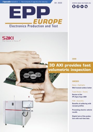
COVER Saki’s 3Xi-M110
COVER Saki’s 3Xi-M110 AXI system. Source: Saki Corporation 22 EPP EUROPE April 2020
COVER Sliced image by tomosynthesis and planar computed tomography. Source: Saki Corporation ventional X-ray systems typically capture less than 10 views or slices) through the entire PCBA area, including mounted components, solder joints, and even PCB warpage. This makes it possible to perform detailed volumetric and shape inspection on all parts of the PCB or module. After capturing the images, the system accurately reconstructs the slices into the shape of the solder ball and fillet (meniscus) to perform reliable solder inspection. Using this process, the system does not just inspect, it combines layers, measures components and features, determines placement variance and board or substrate warpage, and analyzes the internal structures. Measured solder joints are compared to established tolerances and all types of defects, including head-in-pillow (HiP), are identified and classified. PCT is essential for high accuracy defect detection. Hardware design provides better accuracy and image quality Starting with the right hardware is a key factor to realizing accurate inspection and obtaining perfect 3D images. All of the company’s inspection systems are built on a casted iron frame to maintain a rigid and stable platform. A combination of 1-micron analog linear encoders, servo motors on each axis, complex precision calibration, and the stable and robust hardware structure enables exact positioning, sharp clear images, and ensures that the data results collected and communicated are accurate and reliable. The AXI, 3Xi-M110 footprint is approximately 25 % smaller and 30 % lighter than previous models. With its super compact design and lighter weight, the machine can be installed in any standard building upper floors and easily transported. The machine can handle printed circuit boards that are 50 mm (W) x 140 mm (L) to 360 mm (W) x 330 mm (L) in size. For larger boards, a 2-step capturing and loading process can inspect boards that are 360 mm (W) x 510 mm (L) in size. Advanced applications, such as HiP inspection, have a 20 % faster capture time and are even more accurate. Accurate seamless 3D image reconstruction technology PCT technology provides high resolution in both the horizontal and vertical directions. For each PCB image slice, the AXI system provides completely separated images of the top and bottom sides. Because there are separate images for each field of view (FOV), these images can be reconstructed and connected into one image for a seamless 3D constructed model. Automatic board warpage compensation is performed while the image slices are taken to suppress board warpage. A sturdy platform construction improves accuracy. Source: Saki Corporation EPP EUROPE April 2020 23