

TESTtz
-.,fghfgh
-.,fghfgh

Create successful ePaper yourself
Turn your PDF publications into a flip-book with our unique Google optimized e-Paper software.
ACS712<br />
Fully Integrated, Hall Effect-Based Linear Current Sensor<br />
with 2.1 kVRMS Voltage Isolation and a Low-Resistance Current Conductor<br />
Features and Benefits<br />
▪ Low-noise analog signal path<br />
▪ Device bandwidth is set via the new FILTER pin<br />
▪ 5 µs output rise time in response to step input current<br />
▪ 50 kHz bandwidth<br />
▪ Total output error 1.5% at T A = 25°C, and 4% at –40°C to 85°C<br />
▪ Small footprint, low-profile SOIC8 package<br />
▪ 1.2 mΩ internal conductor resistance<br />
▪ 2.1 kV RMS minimum isolation voltage from pins 1-4 to pins 5-8<br />
▪ 5.0 V, single supply operation<br />
▪ 66 to 185 mV/A output sensitivity<br />
▪ Output voltage proportional to AC or DC currents<br />
▪ Factory-trimmed for accuracy<br />
▪ Extremely stable output offset voltage<br />
▪ Nearly zero magnetic hysteresis<br />
▪ Ratiometric output from supply voltage<br />
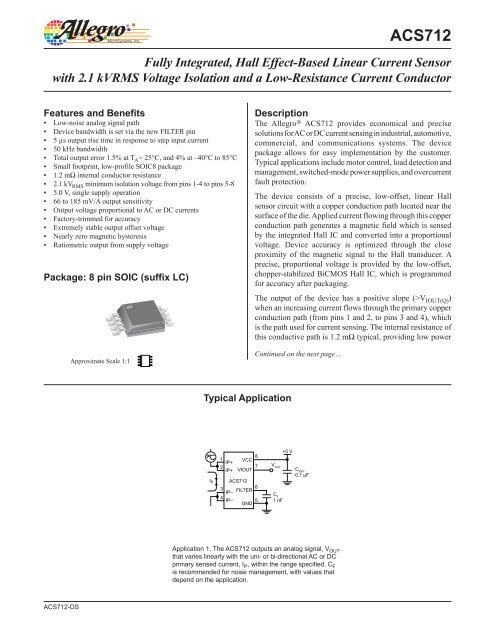
Package: 8 pin SOIC (suffix LC)<br />
Approximate Scale 1:1<br />
Description<br />
The Allegro ® ACS712 provides economical and precise<br />
solutions for AC or DC current sensing in industrial, automotive,<br />
commercial, and communications systems. The device<br />
package allows for easy implementation by the customer.<br />
Typical applications include motor control, load detection and<br />
management, switched-mode power supplies, and overcurrent<br />
fault protection.<br />
The device consists of a precise, low-offset, linear Hall<br />
sensor circuit with a copper conduction path located near the<br />
surface of the die. Applied current flowing through this copper<br />
conduction path generates a magnetic field which is sensed<br />
by the integrated Hall IC and converted into a proportional<br />
voltage. Device accuracy is optimized through the close<br />
proximity of the magnetic signal to the Hall transducer. A<br />
precise, proportional voltage is provided by the low-offset,<br />
chopper-stabilized BiCMOS Hall IC, which is programmed<br />
for accuracy after packaging.<br />
The output of the device has a positive slope (>V IOUT(Q) )<br />
when an increasing current flows through the primary copper<br />
conduction path (from pins 1 and 2, to pins 3 and 4), which<br />
is the path used for current sensing. The internal resistance of<br />
this conductive path is 1.2 mΩ typical, providing low power<br />
Continued on the next page…<br />
Typical Application<br />
1<br />
IP+<br />
2<br />
IP+<br />
8<br />
VCC<br />
7<br />
VIOUT<br />
I P ACS712<br />
3<br />
6<br />
IP–<br />
FILTER<br />
4<br />
IP– 5<br />
GND<br />
V OUT<br />
C F<br />
1 nF<br />
+5 V<br />
C BYP<br />
0.1 µF<br />
Application 1. The ACS712 outputs an analog signal, V OUT .<br />
that varies linearly with the uni- or bi-directional AC or DC<br />
primary sensed current, I P , within the range specified. C F<br />
is recommended for noise management, with values that<br />
depend on the application.<br />
ACS712-DS
ACS712<br />
Fully Integrated, Hall Effect-Based Linear Current Sensor with<br />
2.1 kVRMS Voltage Isolation and a Low-Resistance Current Conductor<br />
Description (continued)<br />
loss. The thickness of the copper conductor allows survival of<br />
the device at up to 5× overcurrent conditions. The terminals of<br />
the conductive path are electrically isolated from the sensor leads<br />
(pins 5 through 8). This allows the ACS712 current sensor to be<br />
used in applications requiring electrical isolation without the use<br />
of opto-isolators or other costly isolation techniques.<br />
The ACS712 is provided in a small, surface mount SOIC8 package.<br />
The leadframe is plated with 100% matte tin, which is compatible<br />
with standard lead (Pb) free printed circuit board assembly processes.<br />
Internally, the device is Pb-free, except for flip-chip high-temperature<br />
Pb‐based solder balls, currently exempt from RoHS. The device is<br />
fully calibrated prior to shipment from the factory.<br />
Selection Guide<br />
Part Number<br />
Packing*<br />
T OP<br />
(°C)<br />
Optimized Range, I P<br />
(A)<br />
Sensitivity, Sens<br />
(Typ) (mV/A)<br />
ACS712ELCTR-05B-T Tape and reel, 3000 pieces/reel –40 to 85 ±5 185<br />
ACS712ELCTR-20A-T Tape and reel, 3000 pieces/reel –40 to 85 ±20 100<br />
ACS712ELCTR-30A-T Tape and reel, 3000 pieces/reel –40 to 85 ±30 66<br />
*Contact Allegro for additional packing options.<br />
Absolute Maximum Ratings<br />
Characteristic Symbol Notes Rating Units<br />
Supply Voltage V CC 8 V<br />
Reverse Supply Voltage V RCC –0.1 V<br />
Output Voltage V IOUT 8 V<br />
Reverse Output Voltage V RIOUT –0.1 V<br />
Output Current Source I IOUT(Source) 3 mA<br />
Output Current Sink I IOUT(Sink) 10 mA<br />
100 total pulses, 250 ms duration each, applied<br />
Overcurrent Transient Tolerance I P at a rate of 1 pulse every 100 seconds.<br />
60 A<br />
Maximum Transient Sensed Current I R (max) Junction Temperature, T J < T J (max) 60 A<br />
Nominal Operating Ambient Temperature T A Range E –40 to 85 ºC<br />
Maximum Junction T J (max) 165 ºC<br />
Storage Temperature T stg –65 to 170 ºC<br />
TÜV America<br />
Certificate Number:<br />
U8V 06 05 54214 010<br />
Parameter<br />
Fire and Electric Shock<br />
Specification<br />
CAN/CSA-C22.2 No. 60950-1-03<br />
UL 60950-1:2003<br />
EN 60950-1:2001<br />
Allegro MicroSystems, Inc.<br />
115 Northeast Cutoff, Box 15036<br />
Worcester, Massachusetts 01615-0036 (508) 853-5000<br />
www.allegromicro.com
ACS712<br />
Fully Integrated, Hall Effect-Based Linear Current Sensor with<br />
2.1 kVRMS Voltage Isolation and a Low-Resistance Current Conductor<br />
Functional Block Diagram<br />
VCC<br />
(Pin 8)<br />
+5 V<br />
Hall Current<br />
Drive<br />
IP+<br />
(Pin 1)<br />
Sense Temperature<br />
Coefficient Trim<br />
IP+<br />
(Pin 2)<br />
IP–<br />
(Pin 3)<br />
IP–<br />
(Pin 4)<br />
Dynamic Offset<br />
Cancellation<br />
Sense<br />
Trim<br />
Signal<br />
Recovery<br />
0 Ampere<br />
Offset Adjust<br />
R F(INT)<br />
VIOUT<br />
(Pin 7)<br />
GND<br />
(Pin 5)<br />
FILTER<br />
(Pin 6)<br />
Pin-out Diagram<br />
IP+<br />
1<br />
8<br />
VCC<br />
IP+<br />
2<br />
7<br />
VIOUT<br />
IP–<br />
3<br />
6<br />
FILTER<br />
IP–<br />
4<br />
5<br />
GND<br />
Terminal List Table<br />
Number Name Description<br />
1 and 2 IP+ Terminals for current being sensed; fused internally<br />
3 and 4 IP– Terminals for current being sensed; fused internally<br />
5 GND Signal ground terminal<br />
6 FILTER Terminal for external capacitor that sets bandwidth<br />
7 VIOUT Analog output signal<br />
8 VCC Device power supply terminal<br />
Allegro MicroSystems, Inc.<br />
115 Northeast Cutoff, Box 15036<br />
Worcester, Massachusetts 01615-0036 (508) 853-5000<br />
www.allegromicro.com
COMMON THERMAL CHARACTERISTICS 1 Min. Typ. Max. Units<br />
ACS712<br />
Fully Integrated, Hall Effect-Based Linear Current Sensor with<br />
2.1 kVRMS Voltage Isolation and a Low-Resistance Current Conductor<br />
COMMON OPERATING CHARACTERISTICS 1 over full range of T OP , C F = 1 nF, and V CC = 5 V, unless otherwise specified<br />
Characteristic Symbol Test Conditions Min. Typ. Max. Units<br />
ELECTRICAL CHARACTERISTICS<br />
Supply Voltage V CC 4.5 5.0 5.5 V<br />
Supply Current I CC V CC = 5.0 V, output open 6 8 11 mA<br />
Output Zener Clamp Voltage V Z I CC = 11 mA, T A = 25°C 6 8.3 – V<br />
Output Resistance R IOUT I IOUT = 1.2 mA, T A =25°C – 1 2 Ω<br />
Output Capacitance Load C LOAD VIOUT to GND – – 10 nF<br />
Output Resistive Load R LOAD VIOUT to GND 4.7 – – kΩ<br />
Primary Conductor Resistance R PRIMARY T A = 25°C – 1.2 – mΩ<br />
RMS Isolation Voltage V ISORMS Pins 1-4 and 5-8; 60 Hz, 1 minute, T A =25°C 2100 – – V<br />
DC Isolation Voltage V ISODC Pins 1-4 and 5-8; 1 minute, T A =25°C – 5000 – V<br />
Propagation Time t PROP I P = I P (max), T A = 25°C, C OUT = open – 3 – μs<br />
Response Time t RESPONSE I P = I P (max), T A = 25°C, C OUT = open – 7 – μs<br />
Rise Time t r I P = I P (max), T A = 25°C, C OUT = open – 5 – μs<br />
Frequency Bandwidth f –3 dB, T A = 25°C; I P is 10 A peak-to-peak 50 – – kHz<br />
Nonlinearity E LIN Over full range of I P – ±1 ±1.5 %<br />
Symmetry E SYM Over full range of I P 98 100 102 %<br />
Zero Current Output Voltage V IOUT(Q) Bidirectional; I P = 0 A, T A = 25°C –<br />
V CC ×<br />
0.5<br />
– V<br />
Magnetic Offset Error V ERROM I P = 0 A, after excursion of 5 A – 0 – mV<br />
Clamping Voltage<br />
V CH Typ. –110 V CC ×<br />
0.9375<br />
V CL Typ. –110 V CC ×<br />
0.0625<br />
Power-On Time t PO<br />
Output reaches 90% of steady-state level, T J = 25°C, 20 A present<br />
on leadframe<br />
Typ. +110 mV<br />
Typ. +110 mV<br />
– 35 – µs<br />
Magnetic Coupling 2 – 12 – G/A<br />
Internal Filter Resistance 3 R F(INT) 1.7 kΩ<br />
1 Device may be operated at higher primary current levels, I P , and ambient, T A , and internal leadframe temperatures, T OP , provided that the Maximum<br />
Junction Temperature, T J (max), is not exceeded.<br />
2 1G = 0.1 mT.<br />
3 R F(INT) forms an RC circuit via the FILTER pin.<br />
Operating Internal Leadframe Temperature T OP E range –40 – 85 °C<br />
Junction-to-Lead Thermal Resistance 2 R θJL Mounted on the Allegro ASEK 712 evaluation board 5 °C/W<br />
Junction-to-Ambient Thermal Resistance R θJA<br />
Mounted on the Allegro 85-0322 evaluation board, includes the power consumed<br />
by the board<br />
1 Additional thermal information is available on the Allegro website.<br />
Value<br />
Units<br />
23 °C/W<br />
2 The Allegro evaluation board has 1500 mm 2 of 2 oz. copper on each side, connected to pins 1 and 2, and to pins 3 and 4, with thermal vias connecting<br />
the layers. Performance values include the power consumed by the PCB. Further details on the board are available from the Frequently Asked<br />
Questions document on our website. Further information about board design and thermal performance also can be found in the Applications Information<br />
section of this datasheet.<br />
Allegro MicroSystems, Inc.<br />
115 Northeast Cutoff, Box 15036<br />
Worcester, Massachusetts 01615-0036 (508) 853-5000<br />
www.allegromicro.com
ACS712<br />
Fully Integrated, Hall Effect-Based Linear Current Sensor with<br />
2.1 kVRMS Voltage Isolation and a Low-Resistance Current Conductor<br />
x05A PERFORMANCE CHARACTERISTICS T OP = –40°C to 85°C 1 , C F = 1 nF, and V CC = 5 V, unless otherwise specified<br />
Characteristic Symbol Test Conditions Min. Typ. Max. Units<br />
Optimized Accuracy Range I P –5 – 5 A<br />
Sensitivity 2 Sens TA Over full range of I P, T A = 25°C – 185 – mV/A<br />
Sens TOP Over full range of I P 178 – 193 mV/A<br />
Noise V NOISE(PP)<br />
Peak-to-peak, T A = 25°C, 185 mV/A programmed Sensitivity,<br />
C F = 47 nF, C OUT = open, 2 kHz bandwidth<br />
Peak-to-peak, T A = 25°C, 185 mV/A programmed Sensitivity,<br />
C F = 4.7 nF, C OUT = open, 20 kHz bandwidth<br />
Peak-to-peak, T A = 25°C, 185 mV/A programmed Sensitivity,<br />
C F = 1 nF, C OUT = open, 50 kHz bandwidth<br />
– 45 – mV<br />
– 20 – mV<br />
– 75 – mV<br />
Electrical Offset Voltage V OE I P = 0 A –40 – 40 mV<br />
Total Output Error 3 E TOT I P =±5 A, T A = 25°C – ±1.5 – %<br />
1 Device may be operated at higher primary current levels, I P , and ambient temperatures, T OP , provided that the Maximum Junction Temperature,<br />
T J(max) , is not exceeded.<br />
2 At –40°C Sensitivity may shift as much 9% outside of the datasheet limits.<br />
3 Percentage of I P , with I P = 5 A. Output filtered.<br />
x20A PERFORMANCE CHARACTERISTICS T OP = –40°C to 85°C 1 , C F = 1 nF, and V CC = 5 V, unless otherwise specified<br />
Characteristic Symbol Test Conditions Min. Typ. Max. Units<br />
Optimized Accuracy Range I P –20 – 20 A<br />
Sensitivity 2 Sens TA Over full range of I P, T A = 25°C – 100 – mV/A<br />
Sens TOP Over full range of I P 97 – 103 mV/A<br />
Noise V NOISE(PP)<br />
Peak-to-peak, T A = 25°C, 100 mV/A programmed Sensitivity,<br />
C F = 47 nF, C OUT = open, 2 kHz bandwidth<br />
Peak-to-peak, T A = 25°C, 100 mV/A programmed Sensitivity,<br />
C F = 4.7 nF, C OUT = open, 20 kHz bandwidth<br />
Peak-to-peak, T A = 25°C, 100 mV/A programmed Sensitivity,<br />
C F = 1 nF, C OUT = open, 50 kHz bandwidth<br />
– 24 – mV<br />
– 10 – mV<br />
– 40 – mV<br />
Electrical Offset Voltage V OE I P = 0 A –30 – 30 mV<br />
Total Output Error 3 E TOT I P =±20 A, T A = 25°C – ±1.5 – %<br />
1 Device may be operated at higher primary current levels, I P , and ambient temperatures, T OP , provided that the Maximum Junction Temperature,<br />
T J (max), is not exceeded.<br />
2 At –40°C Sensitivity may shift as much 9% outside of the datasheet limits.<br />
3 Percentage of I P , with I P = 20 A. Output filtered.<br />
x30A PERFORMANCE CHARACTERISTICS T OP = –40°C to 85°C 1 , C F = 1 nF, and V CC = 5 V, unless otherwise specified<br />
Characteristic Symbol Test Conditions Min. Typ. Max. Units<br />
Optimized Accuracy Range I P –30 – 30 A<br />
Sensitivity 2 Sens TA Over full range of I P , T A = 25°C – 66 – mV/A<br />
Sens TOP Over full range of I P 64 – 68 mV/A<br />
Noise V NOISE(PP)<br />
Peak-to-peak, T A = 25°C, 66 mV/A programmed Sensitivity,<br />
C F = 47 nF, C OUT = open, 2 kHz bandwidth<br />
Peak-to-peak, T A = 25°C, 66 mV/A programmed Sensitivity,<br />
C F = 4.7 nF, C OUT = open, 20 kHz bandwidth<br />
Peak-to-peak, T A = 25°C, 66 mV/A programmed Sensitivity,<br />
C F = 1 nF, C OUT = open, 50 kHz bandwidth<br />
– 20 – mV<br />
– 7 – mV<br />
– 35 – mV<br />
Electrical Offset Voltage V OE I P = 0 A –30 – 30 mV<br />
Total Output Error 3 E TOT I P = ±30 A , T A = 25°C – ±1.5 – %<br />
1 Device may be operated at higher primary current levels, I P , and ambient temperatures, T OP , provided that the Maximum Junction Temperature,<br />
T J (max), is not exceeded.<br />
2 At –40°C Sensitivity may shift as much 9% outside of the datasheet limits.<br />
3 Percentage of I P , with I P = 30 A. Output filtered.<br />
Allegro MicroSystems, Inc.<br />
115 Northeast Cutoff, Box 15036<br />
Worcester, Massachusetts 01615-0036 (508) 853-5000<br />
www.allegromicro.com
ACS712<br />
Fully Integrated, Hall Effect-Based Linear Current Sensor with<br />
2.1 kVRMS Voltage Isolation and a Low-Resistance Current Conductor<br />
Characteristic Performance<br />
I P = 5 A, Sens = 185 mV/A unless otherwise specified<br />
Mean I CC (mA)<br />
Mean Supply Current versus Ambient Temperature<br />
V CC = 5 V<br />
10.0<br />
9.5<br />
9.0<br />
8.5<br />
8.0<br />
7.5<br />
7.0<br />
6.5<br />
6.0<br />
-50 0 50 100 150 200<br />
T A (°C)<br />
I CC (mA)<br />
Supply Current versus Supply Voltage<br />
10.5<br />
10.3<br />
10.1<br />
9.9<br />
9.7<br />
9.5<br />
9.3<br />
9.1<br />
8.9<br />
8.7<br />
8.5<br />
4.5 4.6 4.7 4.8 4.9 5 5.1 5.2 5.3 5.4 5.5<br />
V CC (V)<br />
V ERROM (mV)<br />
Magnetic Offset versus Ambient Temperature<br />
2.00<br />
1.75<br />
1.50<br />
1.25<br />
1.00<br />
0.75<br />
0.50<br />
0.25<br />
0<br />
-50 0 50 100 150 200<br />
T A (°C)<br />
E LIN (%)<br />
Nonlinearity versus Ambient Temperature<br />
I P = 10 A<br />
2.0<br />
1.8<br />
1.6<br />
1.4<br />
1.2<br />
1.0<br />
0.8<br />
0.6<br />
0.4<br />
0.2<br />
0<br />
-50 0 50 100 150 200<br />
T A (°C)<br />
Mean Total Output Error versus Ambient Temperature<br />
I P = 10 A<br />
15.0<br />
Mean E TOT (%)<br />
10.0<br />
5.0<br />
0.0<br />
-5.0<br />
-10.0<br />
-15.0<br />
-50 0 50 100 150 200<br />
T A (°C)<br />
Output Voltage versus Sensed Current<br />
Sensitivity versus Sensed Current<br />
V IOUT (V)<br />
4.5<br />
4.0<br />
3.5<br />
3.0<br />
2.5<br />
2.0<br />
1.5<br />
1.0<br />
0.5<br />
0<br />
-10 -8 -6 -4 -2 0 2 4 6 8 10<br />
Ip (A)<br />
T A (°C)<br />
150<br />
85<br />
25<br />
-40<br />
Sens (mV/A)<br />
188.0<br />
186.0<br />
184.0<br />
182.0<br />
180.0<br />
178.0<br />
176.0<br />
-10 -8 -6 -4 -2 0 2 4 6 8 10<br />
Ip (A)<br />
T A (°C)<br />
85<br />
25<br />
-40<br />
Allegro MicroSystems, Inc.<br />
115 Northeast Cutoff, Box 15036<br />
Worcester, Massachusetts 01615-0036 (508) 853-5000<br />
www.allegromicro.com
ACS712<br />
Fully Integrated, Hall Effect-Based Linear Current Sensor with<br />
2.1 kVRMS Voltage Isolation and a Low-Resistance Current Conductor<br />
Characteristic Performance<br />
I P = 30 A, Sens = 66 mV/A unless otherwise specified<br />
Mean I CC (mA)<br />
Mean Supply Current versus Ambient Temperature<br />
V CC = 5 V<br />
10.0<br />
9.5<br />
9.0<br />
8.5<br />
8.0<br />
7.5<br />
7.0<br />
6.5<br />
6.0<br />
-50 0 50 100 150 200<br />
T A (°C)<br />
Magnetic Offset Current versus Ambient Temperature<br />
I CC (mA)<br />
Supply Current versus Supply Voltage<br />
10.5<br />
10.3<br />
10.1<br />
9.9<br />
9.7<br />
9.5<br />
9.3<br />
9.1<br />
8.9<br />
8.7<br />
8.5<br />
4.5 4.6 4.7 4.8 4.9 5 5.1 5.2 5.3 5.4 5.5<br />
V CC (V)<br />
Nonlinearity versus Ambient Temperature<br />
V ERROM (mV)<br />
1.00<br />
0.80<br />
0.60<br />
0.40<br />
0.20<br />
0<br />
-50 0 50 100 150 200<br />
T A (°C)<br />
E LIN (%)<br />
2.0<br />
1.8<br />
1.6<br />
1.4<br />
1.2<br />
1.0<br />
0.8<br />
0.6<br />
0.4<br />
0.2<br />
0<br />
-50 0 50 100 150 200<br />
T A (°C)<br />
Mean Total Output Error versus Ambient Temperature<br />
Mean E TOT (%)<br />
5.0<br />
4.0<br />
3.0<br />
2.0<br />
1.0<br />
0.0<br />
-1.0<br />
-2.0<br />
-3.0<br />
-4.0<br />
-5.0<br />
-50 0 50 100 150 200<br />
T A (°C)<br />
Output Voltage versus Sensed Current<br />
Sensitivity versus Sensed Current<br />
V IOUT (V)<br />
4.5<br />
4.0<br />
3.5<br />
3.0<br />
2.5<br />
2.0<br />
1.5<br />
1.0<br />
0.5<br />
0<br />
T A (°C)<br />
150<br />
85<br />
25<br />
-40<br />
50.0<br />
-30 -20 -10 0 10 20 30 -30 -20 -10 0 10 20 30<br />
Ip (A)<br />
Ip (A)<br />
Sens (mV/A)<br />
75.0<br />
70.0<br />
65.0<br />
60.0<br />
55.0<br />
T A (°C)<br />
85<br />
25<br />
-40<br />
Allegro MicroSystems, Inc.<br />
115 Northeast Cutoff, Box 15036<br />
Worcester, Massachusetts 01615-0036 (508) 853-5000<br />
www.allegromicro.com
ACS712<br />
Fully Integrated, Hall Effect-Based Linear Current Sensor with<br />
2.1 kVRMS Voltage Isolation and a Low-Resistance Current Conductor<br />
Definitions of Accuracy Characteristics<br />
Sensitivity (Sens). The change in sensor output in response to a<br />
1 A change through the primary conductor. The sensitivity is the<br />
product of the magnetic circuit sensitivity (G / A) and the linear<br />
IC amplifier gain (mV/G). The linear IC amplifier gain is programmed<br />
at the factory to optimize the sensitivity (mV/A) for the<br />
full-scale current of the device.<br />
Noise (V NOISE ). The product of the linear IC amplifier gain<br />
(mV/G) and the noise floor for the Allegro Hall effect linear IC<br />
(≈1 G). The noise floor is derived from the thermal and shot<br />
noise observed in Hall elements. Dividing the noise (mV) by the<br />
sensitivity (mV/A) provides the smallest current that the device is<br />
able to resolve.<br />
Linearity (E LIN ). The degree to which the voltage output from<br />
the sensor varies in direct proportion to the primary current<br />
through its full-scale amplitude. Nonlinearity in the output can be<br />
attributed to the saturation of the flux concentrator approaching<br />
the full-scale current. The following equation is used to derive the<br />
linearity:<br />
∆ gain × % sat ( V<br />
100<br />
{ 1– [<br />
IOUT_full-scale amperes – V IOUT(Q) )<br />
2 (V IOUT_half-scale amperes – V IOUT(Q) )<br />
where V IOUT_full-scale amperes = the output voltage (V) when the<br />
sensed current approximates full-scale ±I P .<br />
Symmetry (E SYM ). The degree to which the absolute voltage<br />
output from the sensor varies in proportion to either a positive<br />
or negative full-scale primary current. The following formula is<br />
used to derive symmetry:<br />
100 V IOUT_+ full-scale amperes – V IOUT(Q)<br />
V IOUT(Q) – V IOUT_–full-scale amperes<br />
<br />
Quiescent output voltage (V IOUT(Q) ). The output of the sensor<br />
when the primary current is zero. For a unipolar supply voltage,<br />
it nominally remains at V CC ⁄ 2. Thus, V CC = 5 V translates into<br />
V IOUT(Q) = 2.5 V. Variation in V IOUT(Q) can be attributed to the<br />
resolution of the Allegro linear IC quiescent voltage trim and<br />
thermal drift.<br />
Electrical offset voltage (V OE ). The deviation of the device output<br />
from its ideal quiescent value of V CC / 2 due to nonmagnetic<br />
causes. To convert this voltage to amperes, divide by the device<br />
sensitivity, Sens.<br />
Accuracy (E TOT ). The accuracy represents the maximum deviation<br />
of the actual output from its ideal value. This is also known<br />
as the total ouput error. The accuracy is illustrated graphically in<br />
the output voltage versus current chart at right.<br />
<br />
{ [<br />
Accuracy is divided into four areas:<br />
• 0 A at 25°C. Accuracy of sensing zero current flow at 25°C,<br />
without the effects of temperature.<br />
• 0 A over Δ temperature. Accuracy of sensing zero current<br />
flow including temperature effects.<br />
• Full-scale current at 25°C. Accuracy of sensing the full-scale<br />
current at 25°C, without the effects of temperature.<br />
• Full-scale current over Δ temperature. Accuracy of sensing fullscale<br />
current flow including temperature effects.<br />
Ratiometry. The ratiometric feature means that its 0 A output,<br />
V IOUT(Q) , (nominally equal to V CC /2) and sensitivity, Sens, are<br />
proportional to its supply voltage, V CC . The following formula is<br />
used to derive the ratiometric change in 0 A output voltage,<br />
ΔV IOUT(Q)RAT (%).<br />
100 V IOUT(Q)VCC / V IOUT(Q)5V<br />
V CC / 5 V <br />
The ratiometric change in sensitivity, ΔSens RAT (%), is defined as:<br />
–I P (A)<br />
I P(min)<br />
Sens VCC / Sens 5V<br />
100<br />
‰ V CC / 5 V <br />
Output Voltage versus Sensed Current<br />
Accuracy at 0 A and at Full-Scale Current<br />
Accuracy<br />
Over<br />
Temp erature<br />
Accuracy<br />
25°C Only<br />
Accuracy<br />
25°C Only<br />
Accuracy<br />
Over<br />
Temp erature<br />
Increasing V IOUT (V)<br />
0 A<br />
Average<br />
V IOUT<br />
Accuracy<br />
25°C Only<br />
Full Scale<br />
I P(max)<br />
Accuracy<br />
Over<br />
Temp erature<br />
+I P (A)<br />
Decreasing V IOUT (V)<br />
Allegro MicroSystems, Inc.<br />
115 Northeast Cutoff, Box 15036<br />
Worcester, Massachusetts 01615-0036 (508) 853-5000<br />
www.allegromicro.com
ACS712<br />
Fully Integrated, Hall Effect-Based Linear Current Sensor with<br />
2.1 kVRMS Voltage Isolation and a Low-Resistance Current Conductor<br />
Definitions of Dynamic Response Characteristics<br />
Propagation delay (t PROP ). The time required for the sensor<br />
output to reflect a change in the primary current signal. Propagation<br />
delay is attributed to inductive loading within the linear IC<br />
package, as well as in the inductive loop formed by the primary<br />
conductor geometry. Propagation delay can be considered as a<br />
fixed time offset and may be compensated.<br />
I (%)<br />
90<br />
0<br />
Primary Current<br />
Transducer Output<br />
Propagation Time, t PROP<br />
t<br />
Response time (t RESPONSE ). The time interval between<br />
a) when the primary current signal reaches 90% of its final<br />
value, and b) when the sensor reaches 90% of its output<br />
corresponding to the applied current.<br />
I (%)<br />
90<br />
0<br />
Primary Current<br />
Transducer Output<br />
Response Time, t RESPONSE<br />
t<br />
Rise time (t r ). The time interval between a) when the sensor<br />
reaches 10% of its full scale value, and b) when it reaches 90%<br />
of its full scale value. The rise time to a step response is used to<br />
derive the bandwidth of the current sensor, in which ƒ(–3 dB) =<br />
0.35 / t r . Both t r and t RESPONSE are detrimentally affected by eddy<br />
current losses observed in the conductive IC ground plane.<br />
I (%)<br />
90<br />
10<br />
0<br />
Primary Current<br />
Transducer Output<br />
Rise Time, t r<br />
t<br />
t PO (µs)<br />
Power on Time versus External Filter Capacitance<br />
200<br />
180<br />
160<br />
I P =5 A<br />
140<br />
120<br />
I<br />
100<br />
P =0 A<br />
80<br />
60<br />
40<br />
20<br />
0<br />
0 10 20 30 40 50<br />
C F (nF)<br />
Step Response<br />
T A =25°C<br />
Output (mV)<br />
1000<br />
Noise versus External Filter Capacitance<br />
15 A<br />
Excitation Signal<br />
Noise (p-p) (mA)<br />
100<br />
10<br />
t r (µs)<br />
1<br />
0.01 0.1 1 10 100 1000<br />
C F (nF)<br />
Rise Time versus External Filter Capacitance<br />
1200<br />
1000<br />
800<br />
600<br />
}<br />
400<br />
200<br />
Expanded in chart at right<br />
0<br />
0 100 200 300 400 500<br />
C F (nF)<br />
C F (nF)<br />
t r (µs)<br />
0 6.647<br />
1 7.74<br />
4.7 17.38<br />
10 32.09087<br />
22 68.15<br />
47 88.18<br />
100 291.26<br />
220 623.02<br />
470 1120<br />
t r (µs)<br />
Rise Time versus External Filter Capacitance<br />
400<br />
350<br />
300<br />
250<br />
200<br />
150<br />
0<br />
0 50 75 100 125 150<br />
C F (nF)<br />
Allegro MicroSystems, Inc.<br />
115 Northeast Cutoff, Box 15036<br />
Worcester, Massachusetts 01615-0036 (508) 853-5000<br />
www.allegromicro.com
ACS712<br />
Fully Integrated, Hall Effect-Based Linear Current Sensor with<br />
2.1 kVRMS Voltage Isolation and a Low-Resistance Current Conductor<br />
Chopper Stabilization Technique<br />
Chopper Stabilization is an innovative circuit technique that is<br />
used to minimize the offset voltage of a Hall element and an associated<br />
on-chip amplifier. Allegro patented a Chopper Stabilization<br />
technique that nearly eliminates Hall IC output drift induced<br />
by temperature or package stress effects. This offset reduction<br />
technique is based on a signal modulation-demodulation process.<br />
Modulation is used to separate the undesired dc offset signal from<br />
the magnetically induced signal in the frequency domain. Then,<br />
using a low-pass filter, the modulated dc offset is suppressed<br />
while the magnetically induced signal passes through the filter.<br />
As a result of this chopper stabilization approach, the output<br />
voltage from the Hall IC is desensitized to the effects of temperature<br />
and mechanical stress. This technique produces devices that<br />
have an extremely stable Electrical Offset Voltage, are immune to<br />
thermal stress, and have precise recoverability after temperature<br />
cycling.<br />
This technique is made possible through the use of a BiCMOS<br />
process that allows the use of low-offset and low-noise amplifiers<br />
in combination with high-density logic integration and sample<br />
and hold circuits.<br />
Hall Element<br />
Regulator<br />
Clock/Logic<br />
Amp<br />
Sample and<br />
Hold<br />
Concept of Chopper Stabilization Technique<br />
Low-Pass<br />
Filter<br />
Typical Applications<br />
+5 V<br />
V PEAK<br />
+5 V<br />
I P<br />
C BYP<br />
0.1 µF<br />
1<br />
IP+<br />
2<br />
IP+<br />
8<br />
VCC<br />
7<br />
VIOUT<br />
ACS712<br />
3<br />
6<br />
IP–<br />
FILTER<br />
4<br />
IP– 5<br />
GND<br />
R F<br />
10 kΩ<br />
+5 V<br />
8<br />
1<br />
IP+<br />
VCC<br />
2<br />
7<br />
IP+ VIOUT<br />
I P ACS712<br />
3 6<br />
IP–<br />
FILTER<br />
4<br />
IP– 5<br />
GND<br />
C OUT<br />
0.1 µF<br />
V OUT<br />
R1<br />
1 MΩ<br />
C F<br />
1 nF<br />
R2<br />
33 kΩ<br />
Application 2. Peak Detecting Circuit<br />
C BYP<br />
0.1 µF<br />
R F<br />
2 kΩ<br />
V OUT<br />
+<br />
–<br />
R1<br />
10 kΩ<br />
C F<br />
1 nF<br />
R3<br />
330 kΩ<br />
C2<br />
0.1 µF<br />
R4<br />
10 kΩ<br />
U1<br />
LT1178<br />
D1<br />
1N4448W<br />
C1<br />
D1<br />
1N914<br />
C1<br />
0.1 µF<br />
V RESET<br />
Q1<br />
2N7002<br />
A-to-D<br />
Converter<br />
Application 4. Rectified Output. 3.3 V scaling and rectification application<br />
for A-to-D converters. Replaces current transformer solutions with simpler<br />
ACS circuit. C1 is a function of the load resistance and filtering desired.<br />
R1 can be omitted if the full range is desired.<br />
C BYP<br />
0.1 µF<br />
R2<br />
+<br />
100 kΩ<br />
1 LM321<br />
8<br />
5<br />
1<br />
IP+<br />
VCC<br />
4<br />
2<br />
7<br />
– 3<br />
IP+ VIOUT<br />
2<br />
R F<br />
I P ACS712<br />
1 kΩ<br />
3<br />
6<br />
R3<br />
IP–<br />
FILTER<br />
3.3 kΩ<br />
C F<br />
4<br />
IP– 5<br />
0.01 µF<br />
GND<br />
C BYP<br />
0.1 µF<br />
+5 V<br />
R1<br />
100 kΩ<br />
8<br />
1<br />
IP+<br />
VCC<br />
2<br />
7<br />
IP+ VIOUT<br />
I P ACS712<br />
3<br />
6<br />
IP–<br />
FILTER<br />
4<br />
IP– 5<br />
GND<br />
R1<br />
33 kΩ<br />
R2<br />
100 kΩ<br />
V OUT<br />
C F<br />
1 nF<br />
4<br />
–<br />
3 +<br />
5<br />
2<br />
1<br />
U1<br />
LMV7235<br />
D1<br />
1N914<br />
V OUT<br />
C1<br />
1000 pF<br />
Application 3. This configuration increases gain to 610 mV/A<br />
(tested using the ACS712ELC-05A).<br />
R PU<br />
100 kΩ<br />
Application 5. 10 A Overcurrent Fault Latch. Fault threshold set by R1 and<br />
R2. This circuit latches an overcurrent fault and holds it until the 5 V rail is<br />
powered down.<br />
Fault<br />
Allegro MicroSystems, Inc.<br />
115 Northeast Cutoff, Box 15036<br />
Worcester, Massachusetts 01615-0036 (508) 853-5000<br />
www.allegromicro.com<br />
10
ACS712<br />
Fully Integrated, Hall Effect-Based Linear Current Sensor with<br />
2.1 kVRMS Voltage Isolation and a Low-Resistance Current Conductor<br />
Improving Sensing System Accuracy Using the FILTER Pin<br />
In low-frequency sensing applications, it is often advantageous<br />
to add a simple RC filter to the output of the sensor. Such a lowpass<br />
filter improves the signal-to-noise ratio, and therefore the<br />
resolution, of the sensor output signal. However, the addition of<br />
an RC filter to the output of a sensor IC can result in undesirable<br />
sensor output attenuation — even for dc signals.<br />
Signal attenuation, ∆V ATT , is a result of the resistive divider<br />
effect between the resistance of the external filter, R F (see<br />
Application 6), and the input impedance and resistance of the<br />
customer interface circuit, R INTFC . The transfer function of this<br />
resistive divider is given by:<br />
⎛ R INTFC ⎞<br />
∆V ATT = V IOUT ⎜<br />
.<br />
R F + R INTFC<br />
⎟<br />
⎝ ⎠<br />
Even if R F and R INTFC are designed to match, the two individual<br />
resistance values will most likely drift by different amounts over<br />
temperature. Therefore, signal attenuation will vary as a function<br />
of temperature. Note that, in many cases, the input impedance,<br />
R INTFC , of a typical analog-to-digital converter (ADC) can be as<br />
low as 10 kΩ.<br />
The ACS712 contains an internal resistor, a FILTER pin connection<br />
to the printed circuit board, and an internal buffer amplifier.<br />
With this circuit architecture, users can implement a simple<br />
RC filter via the addition of a capacitor, C F (see Application 7)<br />
from the FILTER pin to ground. The buffer amplifier inside of<br />
the ACS712 (located after the internal resistor and FILTER pin<br />
connection) eliminates the attenuation caused by the resistive<br />
divider effect described in the equation for ∆V ATT . Therefore, the<br />
ACS712 device is ideal for use in high-accuracy applications<br />
that cannot afford the signal attenuation associated with the use<br />
of an external RC low-pass filter.<br />
+5 V<br />
Pin 3 Pin 4<br />
IP– IP–<br />
VCC<br />
Pin 8<br />
Application 6. When a low pass filter is constructed<br />
externally to a standard Hall effect device, a resistive<br />
divider may exist between the filter resistor, R F, and<br />
the resistance of the customer interface circuit, R INTFC .<br />
This resistive divider will cause excessive attenuation,<br />
as given by the transfer function for ∆V ATT .<br />
0.1 F<br />
Dynamic Offset<br />
Cancellation<br />
Voltage<br />
Regulator<br />
Amp<br />
To all subcircuits<br />
Filter<br />
Allegro ACS706<br />
Out<br />
VIOUT<br />
Pin 7<br />
N.C.<br />
Pin 6<br />
R F<br />
Resistive Divider<br />
Input<br />
Application<br />
Interface<br />
Circuit<br />
Low Pass Filter<br />
Gain<br />
Temperature<br />
Coefficient<br />
Offset<br />
C F<br />
1 nF<br />
R INTFC<br />
Trim Control<br />
IP+ IP+<br />
Pin 1 Pin 2<br />
GND<br />
Pin 5<br />
+5 V<br />
VCC<br />
Pin 8<br />
Application 7. Using the FILTER pin<br />
provided on the ACS712 eliminates the<br />
attenuation effects of the resistor divider<br />
between R F and R INTFC , shown in Application<br />
6.<br />
IP+<br />
Pin 1<br />
IP+<br />
Pin 2<br />
IP–<br />
Pin 3<br />
IP–<br />
Pin 4<br />
Hall Current<br />
Drive<br />
Dynamic Offset<br />
Cancellation<br />
Sense Temperature<br />
Coefficient Trim<br />
Sense<br />
Trim<br />
Signal<br />
Recovery<br />
0 Ampere<br />
Offset Adjust<br />
Buffer Amplifier<br />
and Resistor<br />
Allegro ACS712<br />
VIOUT<br />
Pin 7<br />
Input<br />
Application<br />
Interface<br />
Circuit<br />
R INTFC<br />
GND<br />
Pin 5<br />
FILTER<br />
Pin 6<br />
C F<br />
1 nF<br />
Allegro MicroSystems, Inc.<br />
115 Northeast Cutoff, Box 15036<br />
Worcester, Massachusetts 01615-0036 (508) 853-5000<br />
www.allegromicro.com<br />
11
ACS712<br />
Fully Integrated, Hall Effect-Based Linear Current Sensor with<br />
2.1 kVRMS Voltage Isolation and a Low-Resistance Current Conductor<br />
Package LC, 8-pin SOIC<br />
6.20<br />
5.80<br />
.244<br />
.228<br />
0.25 [.010] M B M<br />
8<br />
5.00 .197<br />
4.80 .189<br />
A<br />
B<br />
8º<br />
0º<br />
0.25<br />
0.17<br />
.010<br />
.007<br />
A<br />
Preliminary dimensions, for reference only<br />
Dimensions in millimeters<br />
U.S. Customary dimensions (in.) in brackets, for reference only<br />
(reference JEDEC MS-012 AA)<br />
Dimensions exclusive of mold flash, gate burrs, and dambar protrusions<br />
Exact case and lead configuration at supplier discretion within limits shown<br />
Terminal #1 mark area<br />
A<br />
4.00<br />
3.80<br />
.157<br />
.150<br />
1.27<br />
0.40<br />
.050<br />
.016<br />
1<br />
2<br />
0.25 .010<br />
8X<br />
0.10 [.004]<br />
C<br />
SEATING<br />
PLANE<br />
C<br />
SEATING PLANE<br />
GAUGE PLANE<br />
0.51<br />
8X<br />
0.31<br />
.020<br />
.012<br />
0.25 [.010] M C A B<br />
1.27 .050<br />
0.25<br />
0.10<br />
1.75<br />
1.35<br />
.010<br />
.004<br />
.069<br />
.053<br />
Package Branding<br />
Two alternative patterns are used<br />
1<br />
2<br />
3<br />
Text 1<br />
Text 2<br />
Text 3<br />
8<br />
7<br />
6<br />
4<br />
5<br />
ACS712T<br />
RLCPPP<br />
YYWWA<br />
ACS Allegro Current Sensor<br />
712 Device family number<br />
T Indicator of 100% matte tin leadframe plating<br />
R Operating ambient temperature range code<br />
LC Package type designator<br />
PPP Primary sensed current<br />
YY Date code: Calendar year (last two digits)<br />
WW Date code: Calendar week<br />
A Date code: Shift code<br />
ACS712T<br />
RLCPPP<br />
L...L<br />
YYWW<br />
ACS Allegro Current Sensor<br />
712 Device family number<br />
T Indicator of 100% matte tin leadframe plating<br />
R Operating ambient temperature range code<br />
LC Package type designator<br />
PPP Primary sensed current<br />
L...L Lot code<br />
YY Date code: Calendar year (last two digits)<br />
WW Date code: Calendar week<br />
The products described herein are manufactured under one or more<br />
of the following U.S. patents: 5,045,920; 5,264,783; 5,442,283;<br />
5,389,889; 5,581,179; 5,517,112; 5,619,137; 5,621,319; 5,650,719;<br />
5,686,894; 5,694,038; 5,729,130; 5,917,320; and other patents<br />
pending.<br />
Allegro MicroSystems, Inc. reserves the right to make, from time<br />
to time, such departures from the detail specifications as may be<br />
required to permit improvements in the performance, reliability,<br />
or manufacturability of its products. Before placing an order,<br />
the user is cautioned to verify that the information being relied<br />
upon is current. The information included herein is believed to<br />
be accurate and reliable. However, Allegro MicroSystems, Inc.<br />
assumes no responsibility for its use; nor for any infringement of<br />
patents or other rights of third parties which may result from its<br />
use.<br />
Copyright ©2006, Allegro MicroSystems, Inc.<br />
For the latest version of this document, go to our website at:<br />
www.allegromicro.com<br />
Allegro MicroSystems, Inc.<br />
115 Northeast Cutoff, Box 15036<br />
Worcester, Massachusetts 01615-0036 (508) 853-5000<br />
www.allegromicro.com<br />
12


