G130/G131 POINT TO POINT DIAGRAM
G130/G131 POINT TO POINT DIAGRAM
G130/G131 POINT TO POINT DIAGRAM

You also want an ePaper? Increase the reach of your titles
YUMPU automatically turns print PDFs into web optimized ePapers that Google loves.
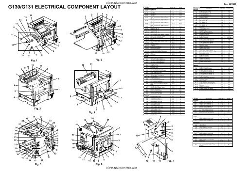
<strong>G130</strong>/<strong>G131</strong> ELECTRICAL COMPONENT LAYOUT<br />
11<br />
10<br />
12<br />
6<br />
4<br />
5<br />
13<br />
7<br />
26<br />
25<br />
24<br />
23<br />
22<br />
21<br />
20<br />
19<br />
18<br />
14<br />
27<br />
8<br />
9<br />
28<br />
17<br />
16<br />
15<br />
9<br />
29<br />
15<br />
8<br />
16<br />
10 11<br />
14<br />
7<br />
Fig. 1<br />
30<br />
Fig. 3<br />
13<br />
Fig. 5<br />
6<br />
12<br />
31<br />
12<br />
1<br />
5<br />
11<br />
32<br />
4<br />
<strong>G130</strong>V203<br />
33<br />
3<br />
1<br />
10<br />
9<br />
2<br />
2<br />
2<br />
3<br />
4<br />
5<br />
6<br />
7<br />
8<br />
3<br />
1<br />
<strong>G130</strong>V201<br />
<strong>G130</strong>V205<br />
18<br />
9<br />
17<br />
16<br />
15<br />
14<br />
18<br />
8<br />
13<br />
10<br />
12<br />
1<br />
19<br />
2<br />
11<br />
Fig. 4<br />
11<br />
20<br />
10<br />
17<br />
7<br />
3<br />
Fig. 2<br />
9<br />
Fig. 6<br />
4<br />
16<br />
6<br />
8<br />
CÓPIA NÃO CONTROLADA<br />
5<br />
15<br />
21<br />
7<br />
5<br />
6<br />
14<br />
6<br />
<strong>G130</strong>V206<br />
5<br />
7<br />
<strong>G130</strong>V202<br />
4<br />
13<br />
<strong>G130</strong>V204<br />
3<br />
4<br />
8<br />
1<br />
9<br />
10<br />
11<br />
12<br />
1<br />
2<br />
3<br />
2<br />
CÓPIA NÃO CONTROLADA<br />
Symbol Description Index No. P-to-P<br />
Printed Circuit Boards<br />
PCB1 LD Unit-Y 1-1 G16<br />
PCB2 LD Unit-K 1-2 G15<br />
PCB3 LD Unit-M 1-3 G14<br />
PCB4 LD Unit-C 1-4 G14<br />
PCB5<br />
Laser Synchronizing Detector Board-<br />
CM – S<br />
1-5 E14<br />
PCB6<br />
Laser Synchronizing Detector Board-<br />
CM – E<br />
1-8 E14<br />
PCB7<br />
Laser Synchronizing Detector Board-<br />
KY – S<br />
1-11 E15<br />
PCB8<br />
Laser Synchronizing Detector Board-<br />
KY – E<br />
1-15 E16<br />
PCB9 Memory Chip – K 2-3 J7<br />
PCB10 Memory Chip – Y 2-4 H11<br />
PCB11 Memory Chip – C 2-5 H11<br />
PCB12 Memory Chip – M 2-6 H10<br />
PCB13 High Voltage Supply Board - Transfer 3-2 F8<br />
PCB14 Paper Width Detection Board 4-3 J6<br />
PCB15 PSU (Power Supply Unit) 6-6 B6<br />
PCB16 DRB 6-12 G5<br />
PCB17 High Voltage Supply Board - C, B 6-13 G9<br />
PCB18 BCU 6-15 I9<br />
PCB19 Operation Panel 1-16 J13<br />
PCB20 SUB PSU 6-14 A3<br />
PCB21 Duplex Control Board 7-5 C10<br />
PCB22 Duplex Drive Board 7-11 B10<br />
PCB23 Transfer Rotation Encoder 3-4 F7<br />
PCB24 Polygon Mirror Motor Drive Board 1-12 F12<br />
PCB25 HDD 6-16 K1<br />
PCB26<br />
Motors<br />
Controller 6-17 J2<br />
M1 Paper Cooling Fan Motor 5-19 J3<br />
M2 3rd Mirror Positioning Motor-M 1-7 G12<br />
M3 3rd Mirror Positioning Motor-C 1-9 G12<br />
M4 3rd Mirror Positioning Motor-Y 1-10 G12<br />
M5 Polygon Motor 1-13 E12<br />
M6 Air Pump – CK 2-2 J8<br />
M7 Air Pump – MY 2-7 J8<br />
M8 Transfer Unit Drive Motor 3-6 F7<br />
M9 Development Drive Motor-CMY 5-1 F6<br />
M10 Drum Drive Motor-CMY 5-4 H6<br />
M11 Paper Feed Motor 5-9 H5<br />
M12 Transfer Belt Contact Motor 5-11 J8<br />
M13,14 Tray Lift Motor 5-13 J12<br />
M15 Drum Drive Motor-K 5-27 H5<br />
M16 Development Drive Motor-K 5-30 F6<br />
M17 PSU Cooling Fan Motor 1 6-5 E2<br />
M18<br />
Laser Optics Housing Cooling Fan<br />
Motor<br />
6-18 J9<br />
M19 Fusing Fan Motor 6-19 F2<br />
M20 Waste Toner Vibration Motor 5-25 J4<br />
M21 Duplex Feed Motor 7-10 A11<br />
M22 Duplex Inverter Motor 1 7-4 D10<br />
M23 Duplex Inverter Motor 2 7-8 D9<br />
M24<br />
Clutches<br />
PCU Cooling FAN Motor 2 6-3 E2<br />
CL1 By-pass Feed Clutch 4-1 J6<br />
CL2 Development Clutch-C 5-2 J3<br />
CL3 Toner Supply Clutch-C 5-3 J5<br />
CL4 Development Clutch-M 5-5 J7<br />
CL5 Toner Supply Clutch-M 5-6 J7<br />
CL6 Registration Clutch 5-7 J10<br />
CL7 Tray 1 Paper Feed Clutch 5-8 J10<br />
CL8 Tray 2 Paper Feed Clutch 5-10 J10<br />
CL9 Toner Supply Clutch-Y 5-23 J5<br />
CL10 Development Clutch-Y 5-24 J3<br />
CL11 Toner Supply Clutch-K 5-26 J5<br />
CL12 Fusing Clutch 5-28 F2<br />
13 7<br />
12<br />
11<br />
1<br />
2<br />
3<br />
4<br />
5<br />
6<br />
8<br />
9<br />
<strong>G130</strong>V207<br />
10 Fig. 7<br />
Symbol<br />
Sensors<br />
Description Index No. P-to-P<br />
S1 Paper Overflow Sensor 6-21 D2<br />
S2 Toner End Sensor – M 2-11 J11<br />
S3 Toner End Sensor – C 2-13 J11<br />
S4 Toner End Sensor – Y 2-15 J11<br />
S5 Humidity Sensor 2-16 J16<br />
S6 Toner End Sensor – K 2-17 J6<br />
S7 TD Sensor – M 2-18 J7<br />
S8 TD Sensor – C 2-18 J5<br />
S9 TD Sensor – Y 2-18 J4<br />
S10 TD Sensor – K 2-18 J4<br />
S11 ID Sensor 3-1 G8<br />
S12 Transfer Belt Sensor 3-3 J5<br />
S13 Relay Sensor 4-4 J15<br />
S14 Vertical Transport Sensor 4-6 J10<br />
S15 By-pass Paper End Sensor 4-7 J6<br />
S16 Registration Sensor 4-9 J7<br />
S17,18 Paper End Sensor 4-10 J15, J16<br />
S19,20 Paper Lift Sensor 4-11 J15, J16<br />
S21 Tray 1 Paper Height Sensor 2 5-12 J12<br />
S22 Tray 2 Paper Height Sensor 2 5-12 J9<br />
S23 Tray 1 Paper Height Sensor 1 5-14 J11<br />
S24 Tray 2 Paper Height Sensor 1 5-14 J12<br />
S25 Belt Mark Sensor 3-5 F8<br />
S26 Duplex Feed Sensor 7-12 B11<br />
S27 Waste Toner Sensor 5-22 J3<br />
S28 Drum Gear Position Sensor - K 5-31 J3<br />
S29 Drum Gear Position Sensor - CMY 5-33 J5<br />
S30 Fusing Exit Sensor 6-1 D2<br />
S31 Paper Exit Sensor 6-20 E2<br />
S32 Duplex Exit Sensor 7-1 D11<br />
S33 Duplex Exit Sensor 2 7-2 D11<br />
S34 Duplex Exit Sensor 3 7-13 D11<br />
S35 Duplex Inverter Sensor 7-9 D11<br />
Switches<br />
SW1 Right Door Switch 2-7 J15<br />
SW2 Vertical Transport Switch 4-8 E6<br />
SW3 Tray 2 Paper Size Switch – 4 5-15 J11<br />
SW4 Tray 2 Paper Size Switch – 2 5-16 J11<br />
SW5 Tray 2 Paper Size Switch – 3 5-17 J11<br />
SW6 Tray 2 Paper Size Switch – 1 5-18 J11<br />
SW7 Tray 1 Set Switch 5-20 J15<br />
SW8 Waste Toner Bottle Set Switch 5-21 J3<br />
SW9 Left Door Switch 6-2 D2<br />
SW10 Main Switch 6-4 D6<br />
SW11 Front Door and Left Door Switch 6-7 A7<br />
SW12<br />
Anti-condensation Heater Switch<br />
(Option)<br />
6-11 E6<br />
SW13 Duplex Door Switch 7-6 D10<br />
SW14 Duplex Inverter Unit Switch 7-7 D10<br />
SW15 PCU/Development Unit Set Switch 2-1 K8<br />
Symbol<br />
Solenoids<br />
Description Index No. P-to-P<br />
SOL1 Air Flow Valve Solenoid – M 2-9 J9<br />
SOL2 Air Flow Valve Solenoid – C 2-10 J9<br />
SOL3 Air Flow Valve Solenoid – Y 2-12 J9<br />
SOL4 Air Flow Valve Solenoid – K 2-14 J10<br />
SOL5 By-pass Pick-up Solenoid 4-2 J6<br />
SOL6 Grip Roller Release Solenoid 4-5 J10<br />
SOL7 Exit Junction Gate Solenoid 5-29 F2<br />
SOL8 Duplex Junction Gate Solenoid 7-3 D10<br />
Lamps<br />
L1 Pressure Roller Fusing Lamp 3-7 B2<br />
L2 Heating Roller Fusing Lamp 3-12 B2<br />
Thermistors<br />
TH1 Thermistor 2 1-6 G13<br />
TH2 Thermistor 1 1-14 G13<br />
TH3 Pressure Roller Thermistor 3-9 C1<br />
TH4 Heating Roller Thermistor 3-10 C1<br />
Thermofuse/Stat<br />
THO1 Pressure Roller Thermofuse 3-8 B2<br />
THO2 Heating Roller Thermostat 3-11 B2<br />
Others<br />
CB1 Earth Leakage Circuit Breaker 6-9 A8<br />
CC1 Choke Coil 6-10 A8<br />
H1<br />
Anti-condensation Heater - Tray<br />
(Option)<br />
6-8<br />
Rev. 06/2005<br />
D6