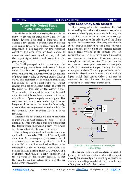
Totem-Pole Output Stage.pub - Tube CAD Journal
Totem-Pole Output Stage.pub - Tube CAD Journal
Totem-Pole Output Stage.pub - Tube CAD Journal

Create successful ePaper yourself
Turn your PDF publications into a flip-book with our unique Google optimized e-Paper software.
<strong>Totem</strong>-<strong>Pole</strong> <strong>Output</strong> <strong>Stage</strong><br />
PSRR Enhancement<br />
In all the push-pull topologies, the goal is the<br />
same: to provide an equal drive signal for the<br />
output devices. This goal is important, as it<br />
ensures a low distortion output signal by forcing<br />
each output device to work equally into the load<br />
impedance, a task required for low distortion<br />
operation. But even when we have labored to<br />
ensure an equal drive signal, we may still find<br />
the output signal tainted with noise from the<br />
power supply.<br />
Don’t all push-pull output stages reject the<br />
power supply noise from their output? Some<br />
come close, but not all push-pull output stages<br />
see a balanced load impedance or an equal share<br />
of power supply noise or are run in true Class-A<br />
mode. This last point is almost never mentioned,<br />
but should be, as the push-pull's two output<br />
devices must be conducting current in order for<br />
the noise to drop out of the output signal.<br />
While at idle, both output devices of a Class-AB<br />
amplifier certainly do draw some current, so the<br />
cancellation of power supply noise is great. But<br />
once any one device stops conducting, it can no<br />
longer work to cancel the noise. Unfortunately,<br />
as amplifiers are only tested for noise at idle, the<br />
real dynamic noise rejection figure is never<br />
measured.<br />
Therefore do not conclude that if an amplifier<br />
is push-pull, it must already be noise rejection<br />
optimized. Thus, our added goal is to understand<br />
the transmission mechanisms used by power<br />
supply noise to make its way to the output.<br />
The techniques outlined in this article are also<br />
applicable to pure tube OTL amplifiers or hybrid<br />
amplifiers. As a consequence, last issue’s use of<br />
a schematic symbol made up of a box with a<br />
capital “N” in it will be retained to illustrate the<br />
universality of the techniques. Once again, this<br />
symbol denotes either a triode, or a pentode, or a<br />
N-channel MOSFET, or a NPN transistor. All<br />
these devices are functionally identical in that<br />
they can be used as output devices in the six<br />
basic output topologies.<br />
Split-Load Unity Gain Circuits<br />
This topology admits two variations. The first<br />
is marked by the cathode side connection, where<br />
the output directly (or, somewhat indirectly, via<br />
a coupling capacitor or a zener or a voltage<br />
regulator) couples to the other side of the phase<br />
splitter’s cathode resistor. Thus, any perturbation<br />
at the output is relayed to the phase splitter’s<br />
plate resistor. How? Since the cathode resistor<br />
sees a fixed voltage at its cathode end, the<br />
perturbation at the amplifier’s output provokes<br />
an increase or decrease of current flowing<br />
through the cathode resistor. This increase or<br />
decrease of current finds only one current path<br />
to the B+ connection: the path through the tube<br />
to the plate resistor. Thus any perturbation at the<br />
output is relayed to the bottom output device’s<br />
input, which then causes either a increase or<br />
decrease in the bottom device’s current<br />
conduction to counter that perturbation.<br />
+300v<br />
input<br />
4k<br />
+250v<br />
+100v<br />
5k<br />
5k<br />
5k<br />
+340v<br />
.33µF<br />
.33µF<br />
N<br />
N<br />
+50v<br />
+100v<br />
output<br />
Split-load, cathode-referenced, unity-gain<br />
output stage<br />
The second topological variation is marked<br />
by a plate side connection, where the output<br />
directly (or indirectly via a coupling capacitor or<br />
a zener or a voltage regulator) couples to the top<br />
of the phase splitter’s plate resistor.<br />
< PREVIOUS Pg. 1<br />
www.tubecad.com Copyright © 2001 GlassWare All Rights Reserved NEXT >
input<br />
4k<br />
10k<br />
+200v<br />
+300v<br />
+100v<br />
.33µF<br />
.33µF<br />
10k<br />
+340v<br />
Thus, any perturbation at the output is<br />
directly relayed to the phase splitter’s plate<br />
resistor. Since the triode’s effective rp is hugely<br />
increased by the unbypassed cathode resistor,<br />
the full magnitude of the perturbation at the<br />
output is relayed to the bottom output device<br />
unattenuated. This error signal provokes either<br />
an increase or a decrease in the current<br />
conduction of the bottom output device in an<br />
effort to cancel the perturbation.<br />
In both topologies, the top output device sees<br />
a constant ground referenced input signal, which<br />
means that the top device will work as hard as<br />
the bottom device to keep the output inline with<br />
the intended signal. Furthermore, in both<br />
topologies, the bottom output device provides no<br />
voltage gain, as all potential gain is entirely fed<br />
back to its input via its connection to the splitload<br />
phase splitter, which results in 100%<br />
degeneration and no gain, just as in the case of a<br />
cathode follower. So, in other words, both output<br />
devices function as followers. When used in a<br />
Class-A amplifier, they effectively equal both<br />
devices placed in parallel, which means a<br />
doubling the transconductance.<br />
B+<br />
2<br />
N<br />
N<br />
B+<br />
output<br />
Split-load, plate-referenced, unity-gain<br />
output stage<br />
For example, a MOSFET based output stage<br />
that used two devices with a transconductance of<br />
1 A/V achieves a 2 A/V input voltage to output<br />
current ratio. If used, however, in a lean Class-<br />
AB or Class-B amplifier, the output stage’s<br />
effective transconductance only equals that of a<br />
single device (or one bank of output devices).<br />
Which topology is better? This was a trick<br />
question, of course: there is not a better topology<br />
without specifying what the intended use is or<br />
what restrictions are placed on the circuit.<br />
For example, if the output devices are<br />
pentodes, then the plate referenced variation is<br />
preferred, as it provides us a means to driving<br />
the top pentode’s screen with the an output<br />
referenced voltage. This was exemplified in the<br />
New York Audio Lab’s versions of the<br />
Futterman OTL amplifier. Using voltage<br />
regulator referenced to the output, these<br />
amplifiers fed the output of the regulators to<br />
both the top output pentode’s screen and to the<br />
plate side of the split-load phase splitter. Thus,<br />
killing two songbirds with one voltage regulator,<br />
if you please. If you pause to think about it, you<br />
will realize that a series voltage regulator is<br />
nothing more than a voltage shifted follower<br />
with the ground as the input source. (In fact,<br />
three-pin voltage regulators can be used as<br />
output devices in an amplifier. The circuit below<br />
shows a single-ended, unity gain, short-circuit<br />
protected amplifier made out two LM317s.)<br />
input<br />
.22µF<br />
100k<br />
adj.<br />
adj.<br />
in<br />
LM317<br />
out<br />
LM317<br />
out<br />
in<br />
output<br />
1M 100k<br />
1.25 1k<br />
+20v<br />
< PREVIOUS Pg. 2<br />
www.tubecad.com Copyright © 2001 GlassWare All Rights Reserved NEXT >
On the other hand, the cathode side<br />
connection can eliminate the need or any extra<br />
components, as the output is usually at ground<br />
level, which allows for DC coupling. Which<br />
circuit to use depends largely on which power<br />
supply noise canceling trick is used.<br />
As both topologies stand in isolation, the<br />
easiest path the power supply noise takes to the<br />
output is from the limitations of either the power<br />
supply shunting capacitor used in the plate side<br />
connection variation or the limitations of the<br />
voltage regulator or signal coupling capacitor<br />
used in the cathode side variation. Should any of<br />
these fail to isolate the power supply noise from<br />
the output stage’s inputs, noise will leak into the<br />
output signal.<br />
But neither topology is used isolation: thus the<br />
input stage often provides a connection to the<br />
power supply noise. Of course, we can strive to<br />
eliminate the power supply noise from polluting<br />
the first stage’s output by using large chokes and<br />
filter capacitors or by even using regulation.<br />
Or we can use the output stage’s common mode<br />
rejection ratio to our advantage.<br />
(The following technique works best with a<br />
Class-A operation mode for the output stage, but<br />
it is still useful with Class-AB output stages.)<br />
Remember that push-pull output stages need to<br />
see a pair of balanced drive signals, i.e. out-ofphase<br />
signals. When the push-pull output stage<br />
is presented with in-phase signals, the output<br />
stage should ideally provide zero amplification.<br />
Thus our goal is to ensure that whatever amount<br />
of power supply noise that leaks through must be<br />
presented to each output device equally in both<br />
phase and amplitude.<br />
The input circuit below realizes an equal<br />
power supply noise distribution by halving the<br />
power supply noise at the first triode’s plate, as<br />
one half noise subtracts from one noise to yield<br />
one half noise at both outputs. This trick requires<br />
that Rk equal (Ra-rp) / (mu + 1), as this is the<br />
only ratio that halves the power supply noise.<br />
Here is a case where the circuit is device<br />
specific, as only a triode will work in the first<br />
tube’s position, as only the triode has a low rp.<br />
300<br />
1M<br />
+150v<br />
Rk<br />
Ra<br />
1M<br />
+ =<br />
+100v<br />
300<br />
+300v<br />
10k<br />
10k<br />
+340v<br />
PS noise balancing front-end<br />
If a pentode or FET is used as the input tube,<br />
then a 50% voltage divider is needed. Two equal<br />
valued resistors will work. The trick will be to<br />
find the value for these resistors that is not so<br />
low as to excessively load the first stage and not<br />
so high as to limit the high frequency response<br />
of the signal leaving the split-load phase splitter.<br />
Understand that this voltage divider will also<br />
divide the audio signal from the first tube. Still<br />
eliminating noise often comes at a price.<br />
(A key point here is that both of these frontend<br />
circuits rely on the first stage seeing the<br />
same amount of noise as does the split-load<br />
phase splitter. Paradoxically, this requirement<br />
might require the removal of some preexisting<br />
power supply filtration circuitry in order to<br />
realize a quieter amplifier.)<br />
This noise rejection optimized front-end has a<br />
wider scope than just hybrid and OTL<br />
amplifiers; it should be used whenever a<br />
grounded cathode amplifier cascades into a splitload<br />
phase splitter; such as is found in the first<br />
half of the Williamson amplifier and even the<br />
Dynaco ST-70 and Mark-3.<br />
2M<br />
4k<br />
to<br />
output<br />
< PREVIOUS Pg. 3<br />
www.tubecad.com Copyright © 2001 GlassWare All Rights Reserved NEXT >
+150v<br />
Ra<br />
100k<br />
+ =<br />
300<br />
4k<br />
+300v<br />
10k<br />
+340v<br />
100% degenerative feedback could eliminate.<br />
(Still, my bet is on local feedback. I just do not<br />
trust a global feedback loop that envelopes<br />
several gain stages. And I worry about the<br />
clipping behavior of the global feedback based<br />
amplifier. Yet I have heard such amplifiers<br />
sound good. More experimentation is needed.)<br />
The circuit bellow is cathode referenced. The<br />
difference between this circuit and the unity-gain<br />
one is that inputs to the output device have been<br />
switched: the top device is driven from the plate<br />
and the bottom device is driven from the<br />
cathode.<br />
300<br />
+75v<br />
+340v<br />
1M<br />
Rk<br />
100k<br />
10k<br />
to<br />
output<br />
Pentode front-end with a resistor voltage divider<br />
Testing this front-end is easy enough: just<br />
ground the input and observe the noise on both<br />
outputs of the phase splitter. Should they differ<br />
in either phase or amplitude, the output stage<br />
will then treat the noise as signal to be<br />
amplified.<br />
Split-Load Gain Circuits<br />
Once again we have two variations to choose<br />
from: plate referenced or cathode referenced. In<br />
both cases we have an output stage that provides<br />
gain at the cost of a much higher output<br />
impedance and a greater distortion figure. In the<br />
previous examples the output devices functioned<br />
as followers, but as they are configured here,<br />
they function as either grounded cathode or<br />
source or emitter amplifiers. But more gain<br />
means more potential feedback, so what we<br />
really have is a zero-sum game, wherein the<br />
feedback can be applied locally or globally.<br />
Which is better? The global feedback network<br />
will provide a lower distortion figure. This is so<br />
because all the feedback can be used to iron out<br />
the most guilty device; whereas its own gain<br />
would set a lower limit to how much distortion<br />
+300v<br />
input<br />
+250v<br />
5k<br />
5k<br />
5k<br />
.33µF<br />
+100v<br />
.33µF<br />
N<br />
N<br />
+50v<br />
output<br />
+100v<br />
Split-load, cathode-referenced, gain output stage<br />
The bottom device is obviously a grounded<br />
“something” amplifier. This is easy to see. But<br />
the top device also looks like it is functioning as<br />
a follower, as the output is taken at its cathode or<br />
source or emitter. The twist lies in the top<br />
device’s input being referenced to the output and<br />
not ground. What difference does this make?<br />
Considered the what happens when the output is<br />
externally forced up 1 volt by a quick going<br />
pulse. When the top device is ground referenced,<br />
the pulse moves the cathode or source or emitter<br />
to become 1 volt less positive than its grid or<br />
gate or base.<br />
< PREVIOUS Pg. 4<br />
www.tubecad.com Copyright © 2001 GlassWare All Rights Reserved NEXT >
Thus the device decreases it conduction equal<br />
to its transconductance, if the idle current was<br />
high enough to absorb that amount that is; or it<br />
ceases to connection altogether, if the idle<br />
current is not high enough. And a negative going<br />
pulse will provoke an increase in conduction<br />
equal to the transconductance of the device. This<br />
is classic follower action in a nutshell.<br />
On the other hand, when the top device is<br />
output referenced, the positive going pulse is<br />
relayed in its entirety to the input of the top<br />
device. In other words, the cathode or source or<br />
emitter may have been bumped up 1 volt, but<br />
then so has the grid or gate or base. And as it is<br />
the voltage relationship between grid and<br />
cathode or gate and source or base and emitter<br />
that controls the flow of current through the<br />
output device, the output device effectively does<br />
not see the pulse. This explains why the output<br />
impedance is so high. (The triode has an<br />
advantage here, as its rp will buck the pulse,<br />
which will offer some output resistance.)<br />
4k<br />
10k<br />
+300v<br />
+200v<br />
+340v<br />
.33µF<br />
+100v<br />
.33µF<br />
10k<br />
N<br />
N<br />
OK, the high output impedance makes sense,<br />
but where does the gain come from when the<br />
load attaches at the cathode or source or emitter?<br />
B+<br />
output<br />
Split-load, plate-referenced, gain output stage<br />
B+<br />
2<br />
The answer is the same place the gain came<br />
from when the load attached to the plate or drain<br />
or collector: the transconductance of the device<br />
gives rise to a change in current flow, which<br />
when this flow also travels through the load,<br />
creates a voltage across the load’s resistance or<br />
impedance. Thus, the rough equation for gain is<br />
gm against the load: gain = gmRL. The top<br />
device sees the same magnitude of input signal<br />
from its input to its output s the bottom device<br />
sees. The only difference is that the bottom<br />
device’s voltage reference is ground and the top<br />
device’s reference is the output of the amplifier.<br />
If the load is a dead short to ground, then both<br />
top and bottom devices become ground<br />
referenced and the drive voltage relationships<br />
become obvious.<br />
Admittedly, when the load impedance is some<br />
value greater than zero, the drive relations<br />
become more difficult to see. Still, as long as we<br />
remember that the reference has moved from<br />
ground to the output, we stand a better chance of<br />
mentally unraveling the drive voltage<br />
relationships. Here is a different example of a<br />
change in reference, in point of view.<br />
A man stands in a large basket-like structure.<br />
In front of him his a small vertical lever that is<br />
labeled “Up” at the top and “Down” at the<br />
bottom. Finding the lever at the mid-position, he<br />
pulls the lever completely up and then<br />
completely down. As he stares at it, the lever has<br />
only traveled half a foot from center to either<br />
extreme. But to the onlookers on the street, who<br />
see a man standing in the container at the end of<br />
fire engine’s crane-ladder, the lever (along with<br />
the man) actually travels 20 ft from one extreme<br />
to the other. Who is right? What is your<br />
reference? If it is that of the man in the basket,<br />
then the lever only moved half a foot from its<br />
center position. If it is that of the onlookers on<br />
the street, then the lever actually moved 10 feet<br />
up (plus the half a foot) and then 10 feet (plus<br />
the half a foot) down from its center position.<br />
After that long recapitulation of how this<br />
circuit works, let’s turn to how the power supply<br />
noise leaks into output in this circuit.<br />
< PREVIOUS Pg. 5<br />
www.tubecad.com Copyright © 2001 GlassWare All Rights Reserved NEXT >
Will the halving of the power supply noise<br />
trick from the circuit work here? Yes, if we<br />
carefully choose the value of capacitor C1, then<br />
the amount of noise at the top of C1 will match<br />
that at the top of 33µF capacitor and the<br />
balancing of the power supply noise will be<br />
assured. These two capacitors cannot share the<br />
same value, as they do not see the same shunt<br />
impedance. The first stage represents a much<br />
lower impedance than the split-load phase<br />
splitter. If the value of resistor Rk is correctly<br />
chosen, then the total effective impedance of this<br />
first stage must equal twice the value of resistor<br />
Ra. Whereas, the split-load phase splitter’s<br />
effective impedance equals rp + (mu + 2)Ra, a<br />
truly huge number. In short, capacitor C1’s<br />
value will have to be somewhat greater than<br />
33µF.<br />
Split-Load and Class-AB<br />
What if we are not willing to pay the price of<br />
high current draw and heat generation that<br />
Class-A demands? The alternative is what<br />
99.9% of power amplifiers run in: Class-AB<br />
operation. (In fact, many (most?) advertised<br />
Class-A amplifiers actually run in Class-AB. If<br />
the amplifier’s output stage does not at least<br />
draw half of the peak output current swing, it is<br />
not Class-A.) Class-AB provides a compromise<br />
between Class-A and Class-B. It is not as<br />
distorting as Class-B and not as inefficient as<br />
Class-A operation.<br />
In fact, many (most?) advertised Class-<br />
A amplifiers actually run in Class-AB. If<br />
the amplifier’s output stage does not<br />
draw at idle at least half of the peak<br />
output current swing, it is not Class-A.<br />
8k<br />
Ra<br />
8k<br />
+300v<br />
33µF C1<br />
+ =<br />
10k<br />
+340v<br />
to<br />
output<br />
Eliminating power supply noise is still possible<br />
within a Class-AB amplifier; it just requires a<br />
little more thought. The circuit below is a case in<br />
point. A bipolar power supply is used and the<br />
output is DC coupled. The bottom output device<br />
must see the same power supply noise at its input<br />
as it does at its connection to the –B connection.<br />
+400v<br />
300<br />
6k<br />
300<br />
1M<br />
+150v 1M<br />
Rk<br />
+100v<br />
2M<br />
10k<br />
input<br />
14k<br />
+340v<br />
+200v<br />
.33µF<br />
N<br />
+40v<br />
PS noise balancing front-end<br />
When the connection is made at the cathode<br />
side, the previous circuit works perfectly, as<br />
both the first stage and the phase splitter share a<br />
common B+ connection. In other words, in this<br />
circuit it does not matter that the output devices<br />
are providing gain.<br />
+98v<br />
+100v<br />
.33µF<br />
14k<br />
0v<br />
N<br />
output<br />
-40v<br />
< PREVIOUS Pg. 6<br />
www.tubecad.com Copyright © 2001 GlassWare All Rights Reserved NEXT >
Introducing this noise at the split-load phase<br />
splitter input ensures that its cathode will relay<br />
the noise faithfully to the bottom device.<br />
Amazingly, the interjection of noise also ensures<br />
that the top device does not see the noise. How<br />
can this be so? The phase splitter’s cathode<br />
resistor sees the same noise signal at both its<br />
ends, thus it never experiences any current<br />
fluctuations due to that noise signal, and thus the<br />
plate resistor cannot reproduce the noise signal.<br />
As it sees a constant current draw from the plate.<br />
6k<br />
+340v<br />
+400v<br />
If the direct connection layout is used instead,<br />
then the path to the negative power supply noise<br />
will be effectively severed. In the circuit below,<br />
a new path is created by connecting a power<br />
supply filter capacitor not output ground but to<br />
the negative power supply rail.<br />
+300v<br />
input<br />
4k<br />
10k<br />
+340v<br />
.33µF<br />
N<br />
+40v<br />
14k<br />
+40v<br />
+100v<br />
+200v<br />
.33µF<br />
N<br />
10k<br />
0v<br />
output<br />
input<br />
+98v<br />
+100v<br />
14k<br />
.33µF<br />
0v<br />
N<br />
-40v<br />
output<br />
If we reverse the connections from the phase<br />
splitter, as in the circuit above, then a different<br />
strategy is required. The bottom device still<br />
needs to see the full negative power supply rail<br />
noise and the top device needs to see no noise.<br />
Both conditions can be satisfied by virtue of the<br />
bipolar power supply. If the phase splitter’s<br />
cathode is noise free, the cathode resistor will<br />
see the full negative power supply noise signal,<br />
which will in turn create a current signal that the<br />
plate resistor will experience. This current signal<br />
Creates an in phase replica of the negative<br />
power supply noise at the plate, which is then<br />
relayed to the bottom output device via the<br />
coupling capacitor. (This trick only works<br />
because the cathode resistor is not grounded.)<br />
4k<br />
.33µF<br />
N<br />
-40v<br />
The split-load phase splitter is marked by an<br />
extremely high plate impedance due to the<br />
presence of the large unbypassed cathode<br />
resistor. Whatever signal appears at the top of<br />
the plate resistor will also appear at the bottom<br />
of the resistor. If this signal meets an inverted<br />
version of its self, both signals will cancel. Thus<br />
if we superimpose the negative power supply<br />
noise on the input signal, the bottom output<br />
device will see the its required noise signal and<br />
the top device will see the null that results from<br />
the input signal being inverted at the plate<br />
canceling the in phase noise signal.<br />
Had the filter capacitor been connected to<br />
ground, the negative power supply noise would<br />
not be canceled at the plate and the output would<br />
polluted by it. The lesson here is that filter<br />
capacitor should not always be terminated into<br />
ground. (Some are not mentally flexible enough<br />
to grasp this and, unfortunately, they design<br />
most amplifiers.)<br />
< PREVIOUS Pg. 7<br />
www.tubecad.com Copyright © 2001 GlassWare All Rights Reserved NEXT >
+300v<br />
+98v<br />
input<br />
4k<br />
10k<br />
+100v<br />
+200v<br />
4k<br />
10k<br />
+340v<br />
.33µF<br />
.33µF<br />
N<br />
N<br />
+40v<br />
output<br />
-40v<br />
Reversing the connections to the phase splitter<br />
requires reversing our strategy. Now the phase<br />
splitter’s cathode needs to see no noise and the<br />
plate needs to see the full negative power supply<br />
rail noise. The filter capacitor’s connection to<br />
the negative power supply rail ensures the<br />
coupling of the rail’s noise to the phase splitter’s<br />
plate and, then via the coupling capacitor, to the<br />
bottom device’s input.<br />
(The 4k resistor that spans the output to the<br />
negative power supply rail only serves to<br />
prevent the phase splitter’s current from being<br />
drawn through the output stage. It could be<br />
eliminated, if desired. It is, however, useful for<br />
allowing testing of the driver stage in isolation<br />
of the output stage.)<br />
I can imagine that some readers are troubled<br />
by the task of superimposing the negative power<br />
supply rail noise on the phase splitter’ input<br />
signal. Just how do you do that? Depending on<br />
the input circuit, several techniques are possible.<br />
For example, a common-cathode amplifier<br />
whose cathode resistor is connected to the<br />
negative power supply rail will find an easy path<br />
to passing the noise to its output, as the signal<br />
present on the cathode resistor will be relayed to<br />
the plate resistor.<br />
0v<br />
Differential Unity Gain Circuit<br />
With the addition of the negative power<br />
supply rail comes a new source of noise. Of<br />
course, a negative power supply is not strictly<br />
required; the long-tail phase splitter only<br />
requires a large valued cathode resistor. The<br />
negative power supply allows for a greater<br />
resistor value; but if the B+ voltage is<br />
sufficiently high, or if a constant current source<br />
used, then need for a negative power supply falls<br />
away. Or does it? If the output stage uses only a<br />
mono-polar power supply, then certainly the<br />
large valued resistor or current source will prove<br />
adequate.<br />
On the other hand, if output stage uses a<br />
bipolar power supply, then the task of noise<br />
elimination becomes more difficult. The<br />
problem lies with the bottom device being<br />
referenced to the negative power supply rail, not<br />
to ground. Thus if the bottom device’s input is<br />
grounded, its cathode or source or emitter will<br />
see the full negative power supply rail noise and<br />
amplify it at its output. On the other hand, if the<br />
bottom device’s input is referenced to the<br />
negative rail, then both its input and its cathode<br />
or source or emitter will see the same noise<br />
signal. But no amplification of the noise ensues.<br />
14k<br />
10k<br />
+200v<br />
14k<br />
10k<br />
+300v<br />
Diff-amp, plate-referenced, unity-gain output stage<br />
B+<br />
.33µF<br />
.33µF<br />
N<br />
N<br />
+200v<br />
B+/2<br />
output<br />
< PREVIOUS Pg. 8<br />
www.tubecad.com Copyright © 2001 GlassWare All Rights Reserved NEXT >
B+<br />
.33µF<br />
.33µF<br />
N<br />
0v<br />
N<br />
output<br />
B-<br />
Now if the power supply rails were truly noise<br />
free, grounding the input to the bottom device<br />
would not result in any noise at the output, as the<br />
ground and the negative rail would both be noise<br />
free. So wouldn’t our efforts be better spent in<br />
trying to cancel the power supply at its source<br />
rather than trying to cleverly cancel it through<br />
circuitry? If the amplifier is run in pure Class-A<br />
mode, the brute force approach has some merit.<br />
But hybrid power amplifier are seldom run in<br />
anything close to pure Class-A and pure tube<br />
OTL amplifier never are, in spite of advertising<br />
copy. What does mode of operation have to do<br />
with noise transmission? More than most tube<br />
gurus know it turns out.<br />
Hybrid and OTL output stages usually run an<br />
idle current of 50 to 200 mA, which translates<br />
into .8 to 3.2 volts into an 8 ohm load. Beyond<br />
these voltages, only one output device delivers<br />
the current into the load. Thus any scheme that<br />
seeks to eliminate power supply noise at the<br />
output by having the noise currents through<br />
bottom output devices cancel ceases to work<br />
beyond this point. Fortunately, the music signal<br />
will tend to mask the noise contribution to the<br />
mix. Now, let’s imagine a power supply that had<br />
no hum. Such a power supply would be greatly<br />
valued when no music was playing, but it would<br />
still give rise to a different type of “noise,” one<br />
that would not show up at idle, but would<br />
manifest itself when play music.<br />
B+<br />
.33µF<br />
.33µF<br />
N<br />
0v<br />
N<br />
output<br />
B-<br />
Power Supply Sag<br />
This “noise” is the collapsing and expanding<br />
of the rail voltage in response to the demands<br />
made on the power supply during the playing of<br />
music. The sag is caused by the greatly varying<br />
current demands the output stage makes on the<br />
power supply, which when multiplied against<br />
the effective series resistance of the power<br />
supply, create a varying power supply rail<br />
voltage. At full output a 100 watt amplifier<br />
draws a peak current of 5A, which results in a 5<br />
volt sag in power supply voltage, if the power<br />
supply’s ESR is 1 ohm; and 25 volts, if the<br />
power supply’s ESR is 5 ohms. (The latter<br />
figure is more likely in an OTL amplifier.) The<br />
ESR is the sum of the diode and transformer<br />
winding resistance; and the higher the power<br />
supply voltage, the greater the ESR.<br />
So even a perfectly quiet power supply can<br />
cause trouble. If the fluctuations in power<br />
supply voltage are not matched in the drive<br />
signal for the bottom device, gross distortions<br />
occur. Imagine a loud passage collapsing the<br />
negative power supply rail, but the DC value of<br />
the drive remains at the idle value. In this<br />
scenario, the cathode or source or emitter has<br />
effectively been made much more positive than<br />
the grid or gate or base, which in turn turns off<br />
the bottom device altogether. Yes feedback will<br />
work to correct the problem, but this means that<br />
the feedback must ease up on its correction of<br />
bandwidth limitations and general distortion<br />
cancellation.<br />
B+<br />
.33µF<br />
.33µF<br />
N<br />
0v<br />
N<br />
output<br />
B-<br />
B+<br />
.33µF<br />
.33µF<br />
N<br />
0v<br />
N<br />
output<br />
B-<br />
< PREVIOUS Pg. 9<br />
www.tubecad.com Copyright © 2001 GlassWare All Rights Reserved NEXT >
And if the amplifier does not use a global<br />
feedback loop, the sound will suffer. Unless, of<br />
course, we match the sagging negative rail<br />
voltage with a negative drive voltage. The circuit<br />
below shows the top device seeing the negative<br />
power supply rail noise reflected to its input,<br />
which will make it to the output. Is the answer to<br />
replace the cathode resistor with a constant<br />
current source?<br />
B+<br />
The solution is to shift the power supply<br />
filtering capacitor connection from ground to the<br />
output stage’s positive rail. A small change in<br />
layout, a large reduction in noise. Now both the<br />
top and bottom device’s see the their required<br />
noise referenced drive voltages. The bottom<br />
device sees the same noise signal as its cathode<br />
or source or emitter sees. Thus without a<br />
difference there cannot be any amplification.<br />
The top device sees the sum of both the positive<br />
and the negative rail noises, which cancel to<br />
null. Once again, nothing to amplify.<br />
B+<br />
B+<br />
input<br />
10k<br />
5k<br />
10k<br />
.33µF<br />
.33µF<br />
N<br />
N<br />
output<br />
0v<br />
input<br />
10k<br />
10k<br />
.33µF<br />
N<br />
B+<br />
output<br />
0v<br />
The circuit below shows the addition of the<br />
constant current source and the inversion of the<br />
noise at the output. What happened? The<br />
constant current source only shifted the source<br />
of the noise to the bottom device.<br />
input<br />
10k<br />
10k<br />
B+<br />
.33µF<br />
.33µF<br />
N<br />
N<br />
B+<br />
B-<br />
output<br />
0v<br />
B-<br />
5k<br />
.33µF<br />
N<br />
The cathode resistor’s value must equal half<br />
the plate resistors value or the noise cancellation<br />
will not occur. Thus the cathode resistor should<br />
not be replaced by a constant current source.<br />
The same holds true for replacing the plate<br />
resistors with current sources. So the answer to<br />
the question, “Are current source a good idea in<br />
tube equipment?” is sometimes yes, sometimes<br />
no, and sometimes it makes no difference.<br />
Look carefully at this last circuit and you will<br />
see that the circuit compensates for power<br />
supply rail sagging and expansion. Should the<br />
negative rail voltage creep upwards, the current<br />
flowing through the cathode resistor will<br />
decrease, which in turn will increase the plate<br />
voltages, as the voltage drop across the plate<br />
resistor will collapse.<br />
B-<br />
< PREVIOUS Pg. 10<br />
www.tubecad.com Copyright © 2001 GlassWare All Rights Reserved NEXT >
In fact, the rail voltage fluctuations are a type<br />
of noise that is induced from dynamic operation<br />
of the amplifier. Unfortunately, most amplifier<br />
tests only evaluate the output at idle and under<br />
steady state output signal conditions, which does<br />
not reveal the dynamic failings of an amplifier.<br />
For example, the sagging of the power supply<br />
rail voltages under a heavy steady current draw<br />
will only initially causes a blocking distortion,<br />
as the bias voltages will eventually catch up with<br />
sagging by on the time constants of the coupling<br />
circuits. Constantly shifting in frequency and in<br />
volume, very little music contains a steady RMS<br />
signal. Thus if the amplifier is always seeing a<br />
sagging and expanding rail voltage and if not<br />
designed to compensate for this fact, it will<br />
always be faltering when faced with music.<br />
Differential Gain Circuit<br />
The output stage can be configured to provide<br />
gain. This is accomplished by bootstrapping the<br />
triode that drives the top output device. This<br />
allows the top output device to realize gain at the<br />
cost of a high output impedance.<br />
input<br />
10k<br />
5k<br />
10k<br />
Replacing the cathode resistor with a constant<br />
current source, once again, does not eliminate<br />
the noise, but interestingly it does not invert the<br />
phase of the noise at the output.<br />
B+<br />
.33µF<br />
.33µF<br />
B+<br />
N<br />
B+<br />
output<br />
0v<br />
N<br />
B-<br />
14k<br />
+200v +200v<br />
10k<br />
+300v<br />
14k<br />
B+<br />
10k<br />
.33µF<br />
N<br />
input<br />
10k<br />
10k<br />
.33µF<br />
N<br />
B+<br />
output<br />
0v<br />
0v<br />
output<br />
.33µF<br />
N<br />
.33µF<br />
N<br />
Eliminating the noise is a bit different in this<br />
circuit compared to the no-gain version. As<br />
shown below, the power supply noise grossly<br />
amplified by the top output device. Here the<br />
cathode resistor relays the negative rail noise to<br />
top device’s input where it is greatly amplified.<br />
B-<br />
Keeping the current source and shifting the<br />
power supply filtering capacitor’s termination<br />
from ground to the negative power supply rail<br />
(as shown below) is the trick to eliminating the<br />
noise. This is another example of how the whole<br />
circuit, the driver circuit and the output stage<br />
and the power supply, must be analyzed to<br />
fruitfully design a power amplifier.<br />
B-<br />
< PREVIOUS Pg. 11<br />
www.tubecad.com Copyright © 2001 GlassWare All Rights Reserved NEXT >
input<br />
10k<br />
10k<br />
Correcting the Long Tail Imbalance<br />
This last circuit holds the answer to a problem<br />
not yet mentioned: the inequality of gain from<br />
each leg of the long-tail phase splitter. In a<br />
nutshell, the first triode realizes more gain than<br />
the second triode, which requires using a larger<br />
valued plate resistor for the second triode.<br />
Why is there an imbalance? The quick answer<br />
is that the common cathode resistor is not<br />
infinite in value. The longer answer is that longtail<br />
phase splitter must present an equal drive<br />
voltage to each triode in order to develop an<br />
equal output gain. But as the first triode’s grid<br />
sees all of the input signal and as the second grid<br />
only sees ground, how is this condition<br />
attainable? First of all, the input grid does not<br />
see all of the signal.<br />
If we look at the first triode carefully we see<br />
that it works as both a cathode follower and a<br />
grounded-cathode amplifier. Of course, if the<br />
cathode followed the grid perfectly, there would<br />
be no grid-to-cathode voltage variation, and thus<br />
no variation in current conduction, and thus no<br />
extra gain at the plate. However, the load that<br />
the cathode works into is not just the common<br />
cathode resistor, but that resistor in parallel with<br />
output impedance of the second triode. In other<br />
words, we have a cathode follower that works<br />
into another cathode follower’s output.<br />
B+<br />
.33µF<br />
.33µF<br />
N<br />
N<br />
B+<br />
output<br />
0v<br />
B-<br />
We begin by making the common cathode<br />
resistor infinitely large. In other words, if it is<br />
infinitely large, we can ignore the cathode<br />
resistor. As both triodes share the same rp , mu,<br />
and plate resistor values, we should expect that<br />
they would also share the same output<br />
impedances. And two equal impedance in series<br />
define a voltage divider that halves any signal.<br />
So if the first grid sees a +2 volt input signal, the<br />
first cathode will only be able to follow half way<br />
and thus see a +1 volt signal. Being grounded,<br />
the second grid sees 0 volts, but the second<br />
cathode sees the same +1 that the first cathode<br />
see, as they are connected. Therefore, the first<br />
triode effectively sees its grid move up 1 volt,<br />
and the second triode effectively sees it grid<br />
move down –1 volt.<br />
So if the common cathode resistor were<br />
infinitely large in value, the gain would match<br />
(actually, they wouldn't, as no cathode follower<br />
has a gain of 1: an imbalance of 1/mu remains).<br />
If it is not, it decreases the voltage division and<br />
thus decreases the input signal the second triode<br />
receives. This explains where the name “long<br />
tail” came from; the larger (the longer) the<br />
common cathode resistor value, the less the<br />
imbalance. Of course, an infinitely large cathode<br />
resistor implies an infinite negative power<br />
supply voltage.<br />
The constant current source frees us from the<br />
need to provide an infinite voltage. Independent<br />
of the voltage across it, it draws a steady current.<br />
Making a constant current source out of<br />
pentodes, FETs, MOSFETs, and transistors is<br />
easier than with a triodes. In this application, the<br />
triode’s chief advantage, rp, becomes a liability,<br />
particularly when high current is needed, as high<br />
current triodes, such as the 6BX7 or 5687, have<br />
very low plate resistances. Still, by using a large<br />
valued cathode resistor, the triode’s effective rp<br />
can be greatly increased. For example, a 6SN7’s<br />
rp is 8k and its mu is 20, which when combined<br />
with a 10k cathode resistor yields an effective rp<br />
of 218k. Put mathematically,<br />
rp´ = (mu + 1)Rk + rp.<br />
< PREVIOUS Pg. 12<br />
www.tubecad.com Copyright © 2001 GlassWare All Rights Reserved NEXT >
Feedback and Gain Imbalance<br />
If a constant current source is not used, the<br />
imbalance can be partially corrected through the<br />
use of a feedback loop. This is the lazy<br />
engineer’s answer to virtually any problem:<br />
noise, limited bandwidth, high output<br />
impedance, and distortion. Design the sloppiest,<br />
cheapest circuit you want, no worry, the<br />
feedback will take care of it. Imagine if a<br />
politician were to argue that every social ill had<br />
one remedy: more laws and more police, one<br />
cop in each business, school, playground,<br />
church, home, and bedroom, if need be. Sad to<br />
say, but it does not require much effort to<br />
imagine such a fool.<br />
input<br />
10k<br />
5k<br />
10k<br />
B+<br />
.33µF<br />
.33µF<br />
N<br />
N<br />
B+<br />
output<br />
0v<br />
In both cases, with feedback and without, the<br />
output devices see the same drive voltage. In the<br />
feedback case, however, the common cathode<br />
resistor sees not the 2 volts of signal, but 38<br />
volts. This huge increase results in a huge<br />
imbalance in drive signals, which the feedback<br />
must work to eliminate.<br />
The feedback must compensate for its use in<br />
this circuit, which means that the feedback<br />
cannot give its all to extending bandwidth or<br />
lowering noise. Remember having 40 dB of<br />
feedback is like having $40,000 in the bank: you<br />
can buy a BMW or a high-end sound system or a<br />
diamond necklace, but not all of them at once.<br />
So it is with feedback, it gets used up.<br />
One solution is not to tie the second grid to<br />
the output and use global feedback that<br />
terminates into the first stage, usually a<br />
grounded-cathode amplifier’s cathode. An<br />
alternative is to use the differential, gain<br />
realizing circuit instead. This topology<br />
demanded the use of a constant current source<br />
for power supply noise elimination and the<br />
current source would also serve to eliminate the<br />
unbalanced drive signals. The circuit below<br />
illustrates the similar drive signals, but what<br />
cannot be seen is the gain imbalance<br />
elimination.<br />
B-<br />
B+<br />
Here we have an interesting example of how a<br />
feedback loop can exacerbate a problem. In the<br />
usual arrangement of the long-tail phase splitter,<br />
the second grid goes to ground. If instead it were<br />
to connect to the output of the totem pole output<br />
stage, then a feedback loop is created. The total<br />
gain of the circuit falls bellow unity, the output<br />
impedance decreases, and the distortion lessens,<br />
but not as much we might expect. Because of the<br />
100% feedback ratio, a much bigger input signal<br />
is needed to bring the output stage to full output.<br />
This means that rather than 4 volts of input<br />
signal, 40 volts of signal might be needed to<br />
drive a tube output stage to 36 volts of output<br />
signal.<br />
input<br />
10k<br />
10k<br />
.33µF<br />
.33µF<br />
N<br />
N<br />
B+<br />
output<br />
0v<br />
B-<br />
< PREVIOUS Pg. 13<br />
www.tubecad.com Copyright © 2001 GlassWare All Rights Reserved NEXT >
Transcendental OTL Remake<br />
As was promised in the issue, we take another<br />
look at the Transcendental OTL amplifier. In<br />
light of what we have covered in both this and<br />
the last issue, we definitively see opportunities<br />
for improvement.<br />
Some readers might be stunned by the hubris<br />
of the last sentence. Do I not realize that the<br />
Transcendental OTL is a Stereophile “Class A”<br />
amplifier? How dare anyone presume to<br />
improve upon perfection?<br />
(I am reminded of when I was in elementary<br />
school my sixth grade teacher told us the brain<br />
teaser about the man who hears a noise outside<br />
is home and fears it might be a bear and runs<br />
outdoors with his rifle. He follows the tracks and<br />
proceeds exactly one mile south, then one mile<br />
east, and then one north, where he finds himself<br />
back home and sees the bear clawing on his<br />
front door. “What color is the bear?” was the<br />
question. The answer is white, which a few of us<br />
gave. The teacher went on to explain that from<br />
only one point on the earth’s surface could one<br />
return home after following the man’s course<br />
and that point was the North <strong>Pole</strong>. I disagreed by<br />
claiming that an infinite number of points<br />
existed that met that condition and that these<br />
points define a circle roughly 4 miles in<br />
circumference. I told him that any point that fell<br />
1 + 1/(2pi) miles north of the South <strong>Pole</strong><br />
qualified, as one mile south, then one mile east,<br />
and then one mile north from any of these points<br />
would bring the man back to his starting point.<br />
The teacher was not amused; the rest of the class<br />
was not amused. Obviously, I did not understand<br />
that the brain teaser was perfect.)<br />
North <strong>Pole</strong><br />
S<br />
N<br />
E<br />
S<br />
South <strong>Pole</strong><br />
E<br />
N<br />
Audio<br />
Gadgets<br />
Shown above is resistor decoding page,<br />
which is only one of ten audio related pages.<br />
Audio Gadgets is software for the<br />
technically minded audiophile. The<br />
quickest way to understand what Audio<br />
Gadgets is all about is to imagine a<br />
programmable calculator designed for the<br />
audio enthusiast.<br />
Audio Gadgets does far too much to fit<br />
in even a 21" monitor; consequently, the<br />
notebook metaphor is used to hold ten<br />
pages of audio topics. Stepped<br />
attenuators to tube circuits.<br />
Windows 3.1/ 95/98/Me/NT<br />
For more information,<br />
please visit our Web site:<br />
GlassWare<br />
www.glass-ware.com<br />
< PREVIOUS Pg. 14<br />
www.tubecad.com Copyright © 2001 GlassWare All Rights Reserved NEXT >
In the world of hi-fi, many believe the notion<br />
that all that can be done in terms of circuit<br />
topology has been done; and thus, the widely<br />
held belief that only improvements in part<br />
quality can lead to improvements in sound<br />
quality. So while the Transcendental OTL is<br />
highly regarded, it certainly is not perfect;<br />
change is possible. Of course, if a recommended<br />
set of changes are great enough, the original<br />
topology disappears. So let’s try to retain as<br />
much as possible of the original amplifier, while<br />
bearing in mind what we have covered so far.<br />
From the last issue, we saw that the patented<br />
drive equalization technique, the bootstrapping<br />
of one of the cathode follower’s B+, used in the<br />
Transcendental OTL was a bust. But we have<br />
seen how to balance the drive signals and<br />
configure the long-tail phase splitter for power<br />
supply noise canceling. Applying these<br />
techniques will require an additional adjustment,<br />
however. The examples of the long-tail phase<br />
splitter based output stages that we have covered<br />
have all assumed that the first grid does not see<br />
any power supply noise. If the grid does see any,<br />
this noise will be amplified along with the<br />
signal. We know that no mater how carefully we<br />
filter the power supply, some power supply will<br />
be superimposed on the input signal to the<br />
output stage. So what we must do is configure<br />
the circuit so that the noise is largely rejected.<br />
input<br />
10k<br />
B+<br />
10k<br />
.33µF<br />
.33µF<br />
0v<br />
B-<br />
Here again is an example of how by<br />
purposely interjecting noise into a circuit we can<br />
lower the noise at the output. Although seldom<br />
mentioned, the long-tail phase splitter, much like<br />
the differential amplifier, contains a good<br />
CMRR mechanism. If both grids see the same<br />
signal, the common signal is barely amplified<br />
compared to the same signal applied to only one<br />
grid. So what is needed (in order to lower the<br />
noise at the output) is to ensure that the second<br />
grid see the same noise that the first stage sees.<br />
input<br />
10k<br />
B+<br />
10k<br />
.33µF<br />
.33µF<br />
How do we balance the noise at both grids in<br />
this amplifier? The 12AX7 based first stage<br />
functions as a voltage divider to the power<br />
supply noise at the top of its plate resistor. In<br />
this instance, the division equals about 30%. In<br />
other words, 10 mV of noise reduces to 3 mV at<br />
the 12AX7’s plate. The same division can be<br />
achieved by using a 70k and a 30k resistors in<br />
series. The problem with using resistors is that<br />
they divide AC and DC voltages equally,<br />
whereas the triode and plate resistor do not, the<br />
DC division being closer to 70%.<br />
Remember we need to ensure that phase<br />
splitter’s both grids see the same DC voltage or<br />
the long-tail phase splitter will not work well if<br />
at all. The solution is found in using two<br />
capacitors in series and a 1M biasing resistor.<br />
The resistor forces the capacitor junction to the<br />
same voltage as the first grid sees.<br />
B-<br />
< PREVIOUS Pg. 15<br />
www.tubecad.com Copyright © 2001 GlassWare All Rights Reserved NEXT >
In the circuit below, the bottom capacitor<br />
equals .1 µF and the top capacitor<br />
equals .047µF. If the values seem reversed,<br />
remember that the reactance of a capacitor is<br />
inversely related to its capacitance. The higher<br />
the capacitance, the lower the reactance. Of<br />
course, the exact values required will probably<br />
differ, but these will be close. Some fiddling is<br />
always needed when canceling noise.<br />
What if the first stage had used a pentode or a<br />
cascode amplifier and the voltage division equal<br />
virtually zero, i.e. all the power supply noise is<br />
present at the plate? In this case, we dispense<br />
with the bottom capacitor altogether.<br />
500v<br />
500v<br />
698k<br />
222v<br />
220k<br />
135v<br />
1M<br />
.047µF<br />
135v<br />
300v<br />
30k<br />
300<br />
1M<br />
.1µF<br />
12AU7<br />
150v<br />
12AU7<br />
12AU7<br />
150v<br />
12AU7<br />
12AX7<br />
100k<br />
3k<br />
15k<br />
.1µF<br />
100k<br />
15k<br />
10<br />
100<br />
1k<br />
10<br />
100<br />
1k<br />
<strong>Tube</strong> <strong>CAD</strong><br />
<strong>Tube</strong> <strong>CAD</strong> does the hard math for you.<br />
This program covers 13 types of tube<br />
circuits, each one divided into four<br />
variations: 52 circuits in all. <strong>Tube</strong> <strong>CAD</strong><br />
calculates the noteworthy results, such as<br />
gain, phase, output impedance, low<br />
frequency cutoff, PSRR, bias voltage, plate<br />
and load resistor heat dissipations. Which<br />
tube gives the most gain? <strong>Tube</strong> <strong>CAD</strong>'s<br />
scenario comparison feature shows which<br />
tube wins.<br />
Windows 3.1/ 95/98/Me/NT<br />
< PREVIOUS Pg. 16<br />
GlassWare<br />
For more information, please visit our Web site :<br />
www.glass-ware.com<br />
www.tubecad.com Copyright © 2001 GlassWare All Rights Reserved NEXT >
The observant reader will have noticed that in<br />
the last schematic that the plate resistor’s value<br />
is much lower than in the original circuit. One<br />
problem with the stock Transcendental OTL is<br />
the ridiculously low plate current for the 12AX7<br />
based input stage: 0.4 mA. Why was this trickle<br />
current chosen? The answer is that the designer<br />
hoped to develop all gain he could out of this<br />
stage. Higher current would have meant a<br />
smaller valued plate resistor and thus less gain.<br />
Why was the extra gain desired? Probably to<br />
lower some of the distortion and to extend the<br />
smaller bandwidth that resulted from using so<br />
little current. Huh? Much like a dog chasing his<br />
tale, we create distortion in the attempt to lower<br />
distortion. Starved of current, a triode produces<br />
more distortion, as it must operate in the bottom,<br />
gooey region of its plate curves. Additionally,<br />
the wimpy current is insufficient to charge the<br />
following stage’s input capacitance (the Miller<br />
effect capacitance) quickly enough to ensure a<br />
wide bandwidth. Our solid-state brothers figured<br />
this out long ago. If an amplifier cannot charge<br />
its internal capacitances quickly enough, the<br />
feedback is going to send the amplifier into a<br />
slew-limiting distortion, e.g. SID.<br />
What’s the solution? Replacing the 12AX7<br />
and 12AU7 with different tubes and increasing<br />
all the idle currents are a good start. <strong>Tube</strong><br />
myopia is a debilitating disease that inflects<br />
more audio designers than can be imagined. (I<br />
remember John Atwood and myself promoting<br />
the 5687, 5965, 6072, and 7062 back in the 80s<br />
and meeting blank stares. I remember being told,<br />
“Don’t you understand, only the 12AU7 and<br />
12AU7 can be used in audio equipment; the<br />
tubes which you like best are meant for<br />
industrial uses and cannot be used in audio<br />
equipment.” Today, I hear, “Only the 300B or<br />
2A3 can be used in a single-ended amplifier.”)<br />
A better choice might be 6N1Ps or 7062s<br />
throughout. These triodes could easily handle<br />
sufficient current to make the amplifier sing. But<br />
I am also troubled by the first stage’s power<br />
supply filtering: just a large valued resistor and a<br />
large valued (22µF) capacitor.<br />
Improving this situation can be easily<br />
accomplished. A shunt regulator can be made<br />
out of the input tube’s unused triode. Or a<br />
constant current draw stage can be made by<br />
adding a cathode follower to the input tube’s<br />
output. For as long as input stage and the<br />
cathode follower shared the same valued load<br />
resistor, their combined current draw will always<br />
equals a constant, as the cathode follower’s<br />
current conduction is in anti-phase to the<br />
grounded-cathode amplifier.<br />
10<br />
10<br />
12AX7<br />
100k<br />
3k<br />
135v<br />
100<br />
350k<br />
222v<br />
220k<br />
135v<br />
12AX7<br />
100k<br />
3k<br />
100<br />
350k<br />
222v<br />
500v<br />
500v<br />
12AX7<br />
1k<br />
220k<br />
to phase spitter<br />
1k<br />
220k<br />
12AX7<br />
to phase spitter<br />
< PREVIOUS Pg. 17<br />
www.tubecad.com Copyright © 2001 GlassWare All Rights Reserved NEXT >
500v<br />
26k<br />
26k<br />
+370v<br />
+370v<br />
20k<br />
300v<br />
200v<br />
34k<br />
200v<br />
34k<br />
300<br />
+450v<br />
1µF 1µF<br />
10µF 10µF<br />
150v<br />
30k<br />
6N1P<br />
.47µF<br />
300<br />
6N1P<br />
3v<br />
6N1P<br />
.1µF<br />
300<br />
6N1P<br />
1µF<br />
100<br />
+170v<br />
100k<br />
6N1P<br />
28k<br />
6N1P<br />
EL509<br />
10<br />
374<br />
5k<br />
to<br />
output<br />
1M<br />
1M<br />
.1µF<br />
47k<br />
47k<br />
-40v<br />
2<br />
output<br />
100<br />
17k<br />
1µF<br />
EL509<br />
x4<br />
-210v<br />
2<br />
-170v<br />
Click on image to see enlargement<br />
The circuit above shows the enhancements<br />
made to the amplifier. As I now look at it, I see<br />
that the 5965 might be a substantially better<br />
choice for the long-tail phase splitter, as it would<br />
provide both more gain and a larger voltage<br />
swing. But then this remake was not meant to<br />
definitive (as I wanted to retain as much of the<br />
original design as possible).<br />
Which of the above modifications yields the<br />
most results? Balancing the drive signals comes<br />
first and is followed by the noise canceling<br />
techniques; and although it is last, using a<br />
different input tube is needed to run a higher idle<br />
current and would have to be implemented.<br />
Conclusions<br />
I remember seeing a circuit that purposely<br />
added hum and limited the bandwidth of solidstate<br />
amplifiers in order to reproduce the golden<br />
sound of tubes! That tube circuits often hum is<br />
as unfortunate as some great wines often<br />
smelling of sulfur dioxide, but only a fool<br />
imagines that sulfates make a grand cru.<br />
Rarely is any topology fully optimized, since<br />
few designers consider noise reduction possible<br />
without the aid of heavy feedback or without<br />
brute force techniques, such as chokes or<br />
regulators. So how can we fairly judge a<br />
topology unless it is completely and competently<br />
designed? Sadly, we can’t.<br />
Do not forget that the techniques outlined<br />
here can be applied to a wholly solid-state<br />
amplifier with a few modifications. So is there<br />
anymore to be squeezed from this topic? I am<br />
sure that there is, but we will wait to see what<br />
the e-mail brings before returning to it.<br />
(I had hope to include an explanation on how<br />
to design a 4 watt OTL amplifier in this article,<br />
but it will have to wait until next time.)<br />
//JRB<br />
Reference<br />
“Analyses of Drivers for Single-Ended Push-<br />
Pull <strong>Stage</strong>,” Hiroshi Amemiya, IRE<br />
Transactions-Audio, Sept-Oct 1955<br />
< PREVIOUS Pg. 18<br />
www.tubecad.com Copyright © 2001 GlassWare All Rights Reserved NEXT >