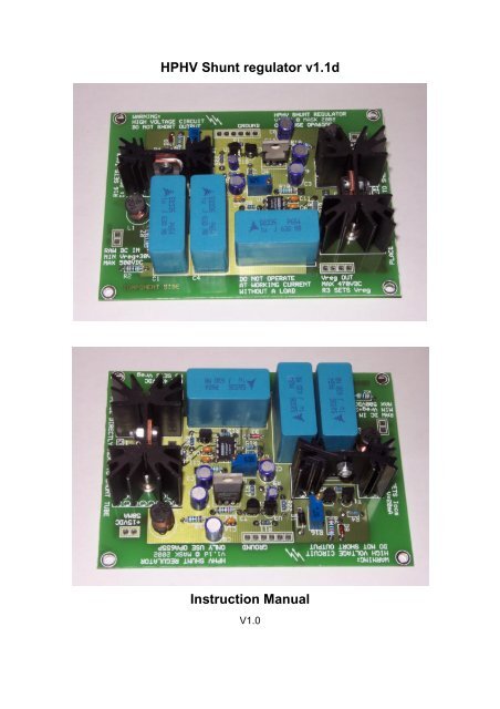
HPHV Shunt regulator v1.1d Instruction Manual - BasAudio.Net
HPHV Shunt regulator v1.1d Instruction Manual - BasAudio.Net
HPHV Shunt regulator v1.1d Instruction Manual - BasAudio.Net

You also want an ePaper? Increase the reach of your titles
YUMPU automatically turns print PDFs into web optimized ePapers that Google loves.
<strong>HPHV</strong> <strong>Shunt</strong> <strong>regulator</strong> <strong>v1.1d</strong><br />
<strong>Instruction</strong> <strong>Manual</strong><br />
V1.0
<strong>HPHV</strong> <strong>Shunt</strong> Regulator <strong>v1.1d</strong> MASK 2002<br />
1 About the <strong>HPHV</strong> shunt <strong>regulator</strong>.......................................3<br />
2 The circuit............................................................................4<br />
3 Before starting.....................................................................9<br />
4 Mounting and soldering the components ......................11<br />
5 Decision time.....................................................................16<br />
6 Warnings............................................................................19<br />
7 Connecting the <strong>regulator</strong> .................................................21<br />
8 Testing and setting up......................................................22<br />
9 Parts list.............................................................................26<br />
10 Schematic .......................................................................27<br />
v1.0 27-12-02 page 2/27
<strong>HPHV</strong> <strong>Shunt</strong> Regulator <strong>v1.1d</strong> MASK 2002<br />
1 About the <strong>HPHV</strong> shunt <strong>regulator</strong><br />
The <strong>HPHV</strong> shunt <strong>regulator</strong> is a very high performance circuit designed to provide a<br />
low impedance power supply for a tube circuit. The circuit is optimized for a constant<br />
phase response within the audioband as well as very low noise.<br />
In order to reduce the stress that tubes face during startup, the <strong>regulator</strong> slowly<br />
raises the output voltage when starting. Full (sonic) stability is reached after about 5<br />
minutes.<br />
The shunt <strong>regulator</strong> has two parts: the constant current source (CCS) and the shunt<br />
(<strong>regulator</strong>). The CCS provides a constant current to the shunt and to the load. In<br />
effect this creates a high impedance (isolation) between the raw dc supply and the<br />
shunt/load.<br />
The shunt regulates the voltage supplied to the load by adjusting the current through<br />
the shunt. The error amp measures the voltage at the shunt/load and compares this<br />
voltage with a reference voltage. If the two voltages differ, the error amp will cause<br />
the shunt to conduct more or less current. This will (re-)set the voltage at the<br />
shunt/load to the correct level. This happens very fast, in fact, much faster than any<br />
audio signal.<br />
Due to the topology, the shunt <strong>regulator</strong> provides a very short path to ground for the<br />
load.<br />
I ccs (I shunt + I load )<br />
+<br />
CCS<br />
I shunt<br />
V reg<br />
I load<br />
RAW<br />
DC<br />
voltage<br />
reference<br />
+<br />
+<br />
-<br />
error amp<br />
shunt<br />
load<br />
ground<br />
v1.0 27-12-02 page 3/27
<strong>HPHV</strong> <strong>Shunt</strong> Regulator <strong>v1.1d</strong> MASK 2002<br />
2 The circuit<br />
The shunt <strong>regulator</strong> basically has two parts: the constant current source and the<br />
shunt.<br />
2.1 The constant current source (CCS)<br />
The CCS consists of T2 and U2. U2 (TL431) is a shunt <strong>regulator</strong> (in a 3 pin device)<br />
that will always try to keep a constant potential (voltage) between its anode and its<br />
reference. It does this by adjusting the potential (voltage) across itself (anodecathode).<br />
T1 and R4 form a CCS (high impedance), so the cathode of U2 is free to move and<br />
well isolated from the raw dc supply. The cathode of U2 sets the bias of T2 (gate<br />
potential through grid stopper R5). So by setting the voltage across itself, U2 sets the<br />
bias of T2 which, in turn, sets the current through R16 & R6. As U2 will try to keep<br />
the voltage between its anode and reference constant, the current through the CCS<br />
is kept constant. This provides high (AC) isolation between the raw dc supply and the<br />
load. In order to function correctly, the CCS needs about 20VDC across it.<br />
The TL431 has a reference voltage of 2.5V. Let’s assume R16 is set midway (50R).<br />
The total resistance of R16 & R6 is 50R + 20R = 70R. U2 will adjust the current so<br />
that it sees 2.5V between its anode and reference. In this case, it will set the current<br />
at 2.5V / 70R = 0.036A (36mA). R6 limits the maximum current at 2.5V / 20R =<br />
0.125A (125mA).<br />
2.2 The shunt<br />
The shunt consists of T4 1 (the shunt) and U1 (the error amp). By setting the gridpotential<br />
of T4, U1 tries to keep the potential (voltage) between its two inputs the<br />
same (it acts on the difference between its two inputs).<br />
The inverting input is connected to a voltage reference, composed of T3 (CCS) and<br />
U3 (shunt reg). The CCS allows the cathode of U3 to move freely and provides a<br />
1 Mosfet shunt option.<br />
v1.0 27-12-02 page 4/27
<strong>HPHV</strong> <strong>Shunt</strong> Regulator <strong>v1.1d</strong> MASK 2002<br />
high impedance (isolation) between U3 and the (regulated) DC rail. The voltage<br />
reference is set at (approximately) 7VDC, so U1 wants to see 7V at its other (noninverting)<br />
input. This input is coupled (AC via C2 and DC via the voltage divider<br />
R19/R18/R3/R17) to the output of the shunt reg (V reg ).<br />
If V reg changes (causing unequal potential between the inputs of U1), U1 will react by<br />
adjusting its output. The output of U1 sets the bias of T4, controlling the current<br />
through the shunt (setting V reg ). The AC coupled input (i.e. error signal) is amplified<br />
about 100 times by U1 (the DC gain is set with R8 and R13). Since U1 (OPA655P)<br />
has a gain-bandwidth product of 240MHz, it is able to handle the signal well beyond<br />
the full audioband, causing very little phase shift within the audioband.<br />
DUE TO THE SPECIAL (DUAL) POWER PINS/CONNECTIONS OF THE OPA655P,<br />
DO NOT SUBSTITUTE THIS DEVICE WITH ANOTHER OPAMP.<br />
The low-end response of the <strong>regulator</strong> is determined by the C2 and R15. The<br />
combination of 1uF and 470K causes a -2dB point below 1Hz. Due to the long RCtime<br />
of C2 and R15, V reg rises very slowly after applying power (prolonging tube life).<br />
At higher frequencies (about >150KHz), the gain of the amp is reduced by C13 so<br />
that the opamp always has ample feedback (providing linearity at these higher<br />
frequencies). In effect, the amp is rolled of with –2dB around 375KHz. At even higher<br />
frequencies, C4 becomes dominant and provides a low impedance path to ground (at<br />
these frequencies, the gain of the opamp is severely reduced by C13). C13 also<br />
damps any potential (HF) oscillation.<br />
v1.0 27-12-02 page 5/27
<strong>HPHV</strong> <strong>Shunt</strong> Regulator <strong>v1.1d</strong> MASK 2002<br />
Simulated response<br />
v1.0 27-12-02 page 6/27
<strong>HPHV</strong> <strong>Shunt</strong> Regulator <strong>v1.1d</strong> MASK 2002<br />
Due to the high gain-bandwidth product of the OPA655, the <strong>regulator</strong> has a very<br />
constant phase angle within the audioband (20-20kHz), The phase-angle is never<br />
more than 2 degrees. I find that excellent phase response is essential to (sonic)<br />
imaging and stability.<br />
This kind of performance can only be achieved by using extraordinary components.<br />
The Burr-Brown OPA655 is a very special amp, definitively never designed to be<br />
used as a error amp in a shunt <strong>regulator</strong> for tube circuits, but it sure does a great job<br />
(BB OPA655 datasheet):<br />
If you want more info on the OPA655, download the datasheet from the Burr-Brown<br />
site:<br />
http://focus.ti.com/docs/prod/productfolder.jhtml?genericPartNumber=OPA655<br />
R8, R13 and C13 form the feedback network for U1 setting the (DC & HF) gain of the<br />
error amp. T5 and R21 form a CCS that force the output of U1 into class A (better<br />
sonics). R1 provides isolation for the output of U1 from the gate capacitance of T4.<br />
v1.0 27-12-02 page 7/27
<strong>HPHV</strong> <strong>Shunt</strong> Regulator <strong>v1.1d</strong> MASK 2002<br />
U4 and its associated parts provide U1 and U3 with clean DC rail. L1 and L2 provide<br />
HF isolation from the raw dc supplies.<br />
In order to monitor the current through the shunt, the voltage at test point I can be<br />
measured. The shunt current (mA) equals this voltage (mV) divided by 10. In order<br />
for the shunt <strong>regulator</strong> to work correctly, the shunt current should be at least 0.2<br />
times the load current.<br />
v1.0 27-12-02 page 8/27
<strong>HPHV</strong> <strong>Shunt</strong> Regulator <strong>v1.1d</strong> MASK 2002<br />
3 Before starting<br />
Before you start soldering, first you have to take care of a bug in the PCB design.<br />
There is a trace on the PCB that really shouldn’t be there (sorry about that ..).<br />
If you look at the picture below, you’ll see which trace has to be cut. You should use<br />
a sharp hobby knife for this. Carefully slice out a 1mm strip of copper.<br />
Use a multimeter (continuity) to check that there is no connection between A and B<br />
(i.e. that the trace has been cut).<br />
To double check things, after mounting R6 check with a multimeter that there is 20<br />
Ohms between points A and B (and not a short).<br />
v1.0 27-12-02 page 9/27
<strong>HPHV</strong> <strong>Shunt</strong> Regulator <strong>v1.1d</strong> MASK 2002<br />
The second thing that has to be taken care of are the ‘ventilation holes’below the<br />
heat sinks. Due to the coating that’s applied to the PCB, the holes are covered with a<br />
thin film, and need to be opened. A toothpick works great.<br />
v1.0 27-12-02 page 10/27
<strong>HPHV</strong> <strong>Shunt</strong> Regulator <strong>v1.1d</strong> MASK 2002<br />
4 Mounting and soldering the components<br />
It is essential to use a small, clean soldering iron (preferably temperature adjustable)<br />
and quality solder. Cut the leads to size before soldering (if you cut them after<br />
soldering you could stress the solder connection). Inspect every solder connection<br />
very carefully (preferably with a magnifying glass).<br />
Some of the solid state components are very sensitive to static charges.<br />
Ground yourself and the soldering iron; place work on grounded (metal)<br />
surface (aluminum foil is fine).<br />
This is from the Burr-Brown OPA655 datasheet:<br />
Due to the very tight layout of the PCB, you should assemble the components in the<br />
following order:<br />
1. Mount C13 (10pF). This cap is mounted on the solder side and soldered<br />
on the component side (the position is marked on the solder side). Make<br />
sure that the leads are short enough so that the opamp can still be<br />
mounted.<br />
v1.0 27-12-02 page 11/27
<strong>HPHV</strong> <strong>Shunt</strong> Regulator <strong>v1.1d</strong> MASK 2002<br />
C13 mounted on solder side<br />
Leads soldered on component side<br />
2. Mount and solder the resistors:<br />
a. R1 30R 0.25W<br />
b. R4 10R 0.25W<br />
c. R5 100R 0.25W<br />
d. R8 200R 0.25W<br />
e. R9 20K 0.25W<br />
f. R11 120R 0.25W<br />
g. R13 20K 0.25W<br />
h. R15 470K 0.25W<br />
i. R17 4K7 0.25W<br />
j. R21 100R 0.25W<br />
k. R22 11K 0.25W<br />
l. R2 300K 0.5W<br />
m. R6 20R 0.5W (check resistance between A and B: 20R)<br />
n. R7 300K 0.5W<br />
o. R10 1K6 0.5W<br />
p. R12 10R 0.5W<br />
q. R14 220R 0.5W<br />
r. R18 150K 0.5W<br />
s. R19 150K 0.5W<br />
v1.0 27-12-02 page 12/27
<strong>HPHV</strong> <strong>Shunt</strong> Regulator <strong>v1.1d</strong> MASK 2002<br />
Resistors mounted and soldered<br />
3. Mount and solder the following parts:<br />
a. D1 1N4007 check correct polarity<br />
b. D3 9.1V zener (marked 55C 9V1) check correct polarity<br />
c. D8 15V zener (marked 55C 15) check correct polarity<br />
d. U1 OPA655P check correct orientation<br />
e. C6 100nF (marked 104)<br />
f. C7 10nF (marked 103)<br />
g. C11 100nF (marked 104)<br />
h. C14 10nF (marked 103)<br />
i. T5 2SK369-V (marked K369) check correct orientation<br />
j. T1 LND150 (marked SiLN D150 check correct orientation<br />
k. U2 TL431 check correct orientation<br />
l. R16 100R trimmer (marked W 101) check correct orientation<br />
m. T3 2SK369-V (marked K369) check correct orientation<br />
n. U3 TL431 check correct orientation<br />
o. C3 33uF 16V check correct polarity<br />
p. C5 10uF 16V check correct polarity<br />
q. R3 5K trimmer (marked W 502) check correct orientation<br />
r. C10 2.2uF 16V check correct polarity<br />
s. U4 LT1085 check correct orientation<br />
v1.0 27-12-02 page 13/27
<strong>HPHV</strong> <strong>Shunt</strong> Regulator <strong>v1.1d</strong> MASK 2002<br />
t. C9 22uF 16V check correct polarity<br />
u. C8 15uF 25V check correct polarity<br />
v. L1 1mH 0.29A (marked 102)<br />
w. L2 2.2mH 0.2A (marked 222)<br />
Small components mounted and soldered<br />
4. Mount and solder the heat sinks. Mount both, flip the PCB over and solder<br />
both the sinks. If you can adjust the temperature of you soldering iron, put it<br />
at about 350C.<br />
5. Now carefully mount the Mosfets T2 and T4 (IRF830). Be sure to put some<br />
heat sink compound between the Mosfets and the heat sink. Mount with<br />
M3 screw and nut, then solder.<br />
6. Mount and solder the big film caps, C1, C2 and C4 (1uF 630V)<br />
v1.0 27-12-02 page 14/27
<strong>HPHV</strong> <strong>Shunt</strong> Regulator <strong>v1.1d</strong> MASK 2002<br />
Completed <strong>HPHV</strong> shunt <strong>regulator</strong> (note the heat sink compound)<br />
7. Check all the solder connections (use a strong light and a magnifier).<br />
8. Check the polarity or orientation of all the semiconductors, electrolytic<br />
capacitors and trimmers. Recheck (its very easy to make a mistake).<br />
v1.0 27-12-02 page 15/27
<strong>HPHV</strong> <strong>Shunt</strong> Regulator <strong>v1.1d</strong> MASK 2002<br />
5 Decision time<br />
It’s time to decide how you’re going to use the shunt <strong>regulator</strong>:<br />
1. Mosfet shunt<br />
2. Tube/mosfet cascode shunt<br />
1. Mosfet shunt<br />
The mosfet shunt is simple. All you need to do is place and solder the jumper on the<br />
solder side marked ‘JUMPER FOR MOSFET SHUNT’(between [C] and [A]). In this<br />
case the Mosfet will handle all the shunt power.<br />
Due to the size of the heat sink, the maximum Mosfet shunt dissipation is 10W.<br />
You can calculate the dissipation: P shunt = V reg * I shunt . I shunt depends on the load<br />
current, and should be at least 0.2 * I load . So if the voltage and current that you need<br />
aren’t very large, a Mosfet shunt will suffice. This will be the case in most preamp<br />
applications.<br />
v1.0 27-12-02 page 16/27
<strong>HPHV</strong> <strong>Shunt</strong> Regulator <strong>v1.1d</strong> MASK 2002<br />
2. Tube/mosfet cascode shunt<br />
If you need more shunt dissipation, then the tube/mosfet cascode shunt option<br />
should be used. In this case, the Mosfet only handles the bias of the shunt tube V bias<br />
(much less than V reg ). The tube will handle V reg minus V bias . Because they are in<br />
series, both the mosfet and the tube carry the same shunt current (I shunt ):<br />
I shunt<br />
I shunt<br />
V reg<br />
no jumper<br />
V bias<br />
With the tube/mosfet cascode option, maximum dissipation depends on the<br />
maximum (plate) power rating of the shunt tube.<br />
For example, say we need V reg =450V and I load =80mA for a power amp. I shunt should<br />
be at least 0.2* I load ; lets use 40mA (0.040A). P shunt = 450 * 0.040 = 18W. We could<br />
use a triode-strapped EL34 as a shunt (EL34: max. 25W anode dissipation).<br />
According to the curves of a triode-strapped EL34 (with 450V anode voltage and<br />
40mA anode current) the grid is at (about) –48V. This bias will be provided by the<br />
Mosfet, which is in series with the tube, so the anode voltage of the EL34 will drop to<br />
about 400V. With 400V and 40mA, the grid of a triode-strapped EL34 is at about –<br />
45V. This will be the bias of the Mosfet (sort of like an auto-bias cathode resistor).<br />
The Mosfet dissipates 45 * 0.04 = 1.8W; the EL34 dissipates 405 * 0.04 = 16,2W.<br />
v1.0 27-12-02 page 17/27
<strong>HPHV</strong> <strong>Shunt</strong> Regulator <strong>v1.1d</strong> MASK 2002<br />
Be sure to put a grid stopper resistor (100R) directly at the socket of the tube.<br />
Mount the shuntreg as close as possible to the shunt tube.<br />
For low noise, be sure to use DC for shunt tube heater (I do not recommend<br />
using a IHT as a shunt tube). Do not float the heater supply, but connect to<br />
ground or (better) raise the heater about +20VDC above V bias .<br />
Make sure DC heater power is applied before RAW DC (allow shunt tube to fully<br />
heat-up).<br />
If the grid biases at less than –20V, the grid may be connected to G0 (else<br />
connect the grid to G1).<br />
v1.0 27-12-02 page 18/27
<strong>HPHV</strong> <strong>Shunt</strong> Regulator <strong>v1.1d</strong> MASK 2002<br />
6 Warnings<br />
As this is a high voltage circuit, you can get a serious jolt (or worse) if you touch the<br />
shunt reg while powered is applied. The heat sinks aren’t isolated, so they can be at<br />
500V.<br />
IF POWER IS SUPPLIED TOT THE REG, DO NOT TOUCH IT.<br />
USE A SMALL ISOLATED SCREWDRIVER TO (CAREFULLY) ADJUST THE<br />
TRIMMERS.<br />
The circuit combines high voltages and very sensitive solid state components. A very<br />
tricky marriage, indeed. During the development of the circuit many solid state<br />
components were destroyed (they blew up and gave their lives to high-end progress).<br />
That experience has helped to make this version of the <strong>regulator</strong> completely stable,<br />
but be very careful when testing and setting up.<br />
Check out the notes on the circuit diagram (page 27).<br />
DO NOT POKE AROUND A LIVE REGULATOR WITH A PROBE.<br />
It’s very easy to slip, make a short and destroy some (very expensive) parts.<br />
If you need to do a measurement, power down the <strong>regulator</strong>, wait 10s for all the<br />
caps to discharge, connect the probes to the <strong>regulator</strong>, set the meter(s), apply<br />
power to the <strong>regulator</strong> and measure. Repeat for each new measurement.<br />
If the output is shorted, (obviously) V reg will go down to ground. C2 is (still) charged<br />
and (still) has a potential of V reg across it. This causes the top of D3 (and the noninverting<br />
input of the OPA655P) to be driven to a potential of –V reg . Luckily when this<br />
happens, D3 acts as a kind of fuse and will ‘hold’the potential at –0.6V (protecting<br />
U1). This causes C3 to very quickly discharge though D3.<br />
v1.0 27-12-02 page 19/27
<strong>HPHV</strong> <strong>Shunt</strong> Regulator <strong>v1.1d</strong> MASK 2002<br />
DO NOT SHORT THE OUTPUT. Should this happen, D3 will probably blow<br />
(protecting the OPA655P). D3 will have to be replaced.<br />
The components and heat sinks used have maximum ratings. These should never be<br />
exceeded.<br />
Do not exceed the maximum voltages of Raw DC (500VDC) and V reg (470VDC).<br />
Do not exceed the maximum CCS (5W) and shunt dissipation (10W).<br />
To calculate the CCS dissipation: P = (V RAW DC – V reg ) * I ccs<br />
To calculate the shunt dissipation: P = V reg * I shunt<br />
ALLOW FOR GOOD VENTILATION OF THE HEAT SINKS. COOL RUNNING<br />
COMPONENTS LAST LONGER.<br />
The maximum load current is 100mA (I ccs = 125mA; I shunt = 25mA). Since V reg is<br />
max 470V, max load dissipation is 470 * 0.1 = 47W. At this setting, the<br />
maximum shunt dissipation is exceeded: Pshunt = 470 * 0.025 = 12W. If you<br />
need this much power, the tube/mosfet cascode shunt option must be used.<br />
DO NOT OPERATE THE REGULATOR AT WORKING CURRENT WITHOUT A<br />
LOAD.<br />
If this happens, the shunt will have to handle ALL the current (I ccs ), exceeding<br />
the maximum dissipation of the heat sink. The heat sink will probably overheat<br />
and components will fail.<br />
The IRF830’s can dissipate a lot of power (75W), but only if properly heat<br />
sinked. If you need more power for the CCS and/or the shunt, you must use<br />
bigger heat sinks (or use the tube/mosfet cascode shunt option).<br />
v1.0 27-12-02 page 20/27
<strong>HPHV</strong> <strong>Shunt</strong> Regulator <strong>v1.1d</strong> MASK 2002<br />
7 Connecting the <strong>regulator</strong><br />
The <strong>regulator</strong> is connected to a (unregulated) +15VDC supply (50mA), a<br />
(unregulated) RAW DC (HV) supply and the load (shunt tube option connections not<br />
shown).<br />
RAW DC IN<br />
+15VDC<br />
Vreg OUT<br />
+ + +<br />
RAW<br />
DC<br />
+15V<br />
DC<br />
GROUND<br />
LOAD<br />
v1.0 27-12-02 page 21/27
<strong>HPHV</strong> <strong>Shunt</strong> Regulator <strong>v1.1d</strong> MASK 2002<br />
8 Testing and setting up<br />
In order to test and setup the <strong>regulator</strong> without harming it, you must follow the<br />
next instructions exactly.<br />
If testing the <strong>regulator</strong> with power applied, always use probes that you can<br />
clamp (hands-off measurement), so that you can’t slip with a probe possibly<br />
causing a short.<br />
First check if the ‘low voltage’section of the circuit works.<br />
Don’t connect the high voltage RAW DC supply yet.<br />
1. Connect a DC supply of 15V (50mA) to +15VDC [+] and GROUND [-], but don’t<br />
apply power yet.<br />
2. Connect a multimeter (set to measure Volts) between G1 [+probe] and GROUND<br />
[-probe] (it helps to solder a small piece of wire to the G1 test-point).<br />
3. Apply power to the 15V supply and check the multimeter. It should read around<br />
10.4V. Also check the temperature of U4 (LT1085) with a finger. You might feel it<br />
warming up a bit, but it should not be very hot.<br />
4. Power down and disconnect the probes.<br />
5. Connect the multimeter (still set to measure Volts) between R8 [+probe] (the side<br />
away from the opamp; right below C7) and GROUND [-probe].<br />
6. Apply power to the 15V supply and check the multimeter. It should read around<br />
7.1V.<br />
7. Power down and disconnect the probes.<br />
8. Connect the multimeter (still set to measure Volts) between R1 [+probe] (either<br />
side of R1) and GROUND [-probe].<br />
9. Apply power to the 15V supply and check the multimeter. It should read around<br />
1.2V. This last measurement indicates that the opamp is working correctly.<br />
10. Power down and disconnect the probes.<br />
v1.0 27-12-02 page 22/27
<strong>HPHV</strong> <strong>Shunt</strong> Regulator <strong>v1.1d</strong> MASK 2002<br />
The next step is essential. Failure to do so may cause components to exceed<br />
their maximum ratings.<br />
With a small screwdriver, turn R16 fully counter clockwise. This may take 10-20<br />
turns. At one point, when turning the adjustment screw, you’ll hear a slight clicking<br />
sound. The trimmer is now at its end-stop. Leave it at this position.<br />
Set a multimeter to measure resistance. Do not apply power.<br />
Measure the resistance between points A and B (the pins of R16). Use non-clamping<br />
probes (i.e. probes with fine/sharp points) for this measurement. The meter should<br />
read (about) 100 Ohms. The CCS is now set for minimum current (around 25mA).<br />
Now check if the high voltage section of the circuit works correctly. For this you need<br />
two multimeters (ideally three so you can measure RAW DC as well).<br />
If you have a variac (or a regulated B+ supply), I recommend using it to slowly raise<br />
the RAW DC when testing.<br />
If you’re using the mosfet shunt option, make sure you’ve mounted and soldered the<br />
jumper (solder side). If you’re using the tube/mosfet cascode shunt option, turn on the<br />
tube heater supply and allow the heater to fully heat-up.<br />
v1.0 27-12-02 page 23/27
<strong>HPHV</strong> <strong>Shunt</strong> Regulator <strong>v1.1d</strong> MASK 2002<br />
1. Connect the first multimeter (set to measure mVolts) between I [+probe] and<br />
GROUND [-probe] (it helps to solder a small piece of wire to I).<br />
2. Connect the second multimeter (set to measure Volts) between V reg [+probe] and<br />
GROUND [-probe] (it helps to solder a small piece of wire to V reg ).<br />
3. Connect the 15VDC supply to +15VDC [+] and GROUND [-], but don’t apply<br />
power yet.<br />
4. Connect the RAW DC supply to RAW B+ [+] and GROUND [-], but don’t apply<br />
power yet.<br />
5. Apply power to the 15VDC supply.<br />
6. Apply power to the RAW DC supply (or if you’re using a variac raise slowly).<br />
7. If all is well, I (the first multimeter) should be at about 250mV (indicating 25mA<br />
shunt current). V reg (the second multimeter) should slowly rise to RAW DC or a<br />
lower value. It will take about 2 minutes for V reg to stabilize.<br />
8. If V reg rises to RAW DC and I decreases, then V reg is set too high.<br />
9. If V reg rises to a value below RAW DC and I remains stable (about 250mV), then<br />
V reg is set too low.<br />
10. Now -slowly- adjust R3 to set V reg to the correct value. Turning R3 clockwise<br />
increases V reg ; turning R3 counterclockwise decreases V reg . Because of the large<br />
RC-time of C2 and R15, it will take some time for V reg to stabilize after adjusting<br />
R3, so adjust R3 one turn at a time, and wait for V reg to settle.<br />
11. V reg should now be set at the correct value. Power down the RAW DC supply and<br />
check that V reg quickly drops. Re-apply power to the RAW DC supply and verify<br />
that V reg slowly rises to the correct value.<br />
12. If you have a scope, check the V reg rail. You should see clean DC.<br />
13. Power down both supplies.<br />
If the above tests have successfully been completed, the <strong>regulator</strong> works. All that<br />
needs to be done now, is to set the shunt current while powering the actual load.<br />
Do not adjust R3 anymore, only R16.<br />
1. Connect the two multimeters like before (I and V reg ).<br />
2. Connect the load to V reg [+] and GROUND [-].<br />
v1.0 27-12-02 page 24/27
<strong>HPHV</strong> <strong>Shunt</strong> Regulator <strong>v1.1d</strong> MASK 2002<br />
3. Apply power to the 15VDC supply and the RAW DC supply.<br />
4. Verify that V reg slowly rises.<br />
5. As V reg rises, I will drop. When I drops, turn R16 clockwise to increase I. Beware<br />
that V reg rises slowly, so allow time to stabilize before adjusting R16.<br />
6. When V reg reaches the value you set it to before, set I to the desired shunt current<br />
(I shunt ).<br />
The <strong>regulator</strong> is now setup for powering the load. Beware that for a different load, you<br />
will need to readjust V reg and I.<br />
v1.0 27-12-02 page 25/27
<strong>HPHV</strong> <strong>Shunt</strong> Regulator <strong>v1.1d</strong> MASK 2002<br />
9 Parts list<br />
Reference Component Description Notes<br />
L1 1mH 0.29A PCB mount HF choke Panasonic ELC series<br />
L2 2.2mH 0.2A PCB mount HF choke Panasonic ELC series<br />
D1 1N4007 Diode 1000V<br />
D8 BZX55C15 15V Zener diode<br />
D3 BZX55C9V1 9.1V Zener diode<br />
T1 LND150N3 HV depletion mode MOSFET Can be replaced by BSS135 (change R4 to 330R)<br />
T2, T4 IRF830 HV MOSFET IRF830: 500V max<br />
T3, T5 2SK369-V JFET Can be replaced by 2SK170-V (Idss > 14mA)<br />
U2, U3 TL431 Programmable shunt <strong>regulator</strong> TO-92<br />
U4 LT1085CT Adjustable <strong>regulator</strong> TO-220<br />
U1 OPA655P Wideband, Unity Gain Stable, FET-Input Op Amp DO NOT SUBSTITUTE OTHER OP AMP<br />
C1, C2, C4 1uF 630V MKP capacitor 27.5mm lead pitch EPCOS, WIMA 27.5mm lead pitch<br />
C5 10uF 16V Electrolytic capacitor Sanyo OSCON SC<br />
C8 15uF 25V Electrolytic capacitor Sanyo OSCON SC<br />
C10 2.2uF 16V Electrolytic capacitor Sanyo OSCON SC<br />
C3 33uF 16V Electrolytic capacitor Sanyo OSCON SC<br />
C9 22UF 16V Electrolytic capacitor Sanyo OSCON SC<br />
C6,C11 100nF 50V Ceramic capacitor X7R 2.5mm lead pitch<br />
C7, C14 10nF 50V Ceramic capacitor X7R 2.5mm lead pitch<br />
C13 10pF Silvered mica 5.7mm lead pitch - mounted on component side<br />
R16 100R Trimmer 25 turn Bourns 3296W series<br />
R3 5K Trimmer 25 turn Bourns 3296W series<br />
R6 20R 0.5W resistor All 0.5W resistors have 7mm package<br />
R18, R19 150K 0.5W resistor<br />
R14 220R 0.5W resistor<br />
R2, R7 300K 0.5W resistor<br />
R10 1K6 0.5W resistor<br />
R12 10R 0.5W resistor<br />
R4 10R 0.25W resistor All 0.25W resistors have 4mm package<br />
R5, R21 100R 0.25W resistor<br />
R11 120R 0.25W resistor<br />
R15 470K 0.25W resistor<br />
R9, R13 20K 0.25W resistor<br />
R22 11K 0.25W resistor<br />
R17 4K7 0.25W resistor<br />
R1 30R 0.25W resistor<br />
R8 200R 0.25W resistor<br />
WE 637 Heat sink 25.4 * 34.9 * 12.7<br />
WE 647 Heat sink 25.4 * 41.9 * 25.4<br />
v1.0 27-12-02 page 26/27
<strong>HPHV</strong> <strong>Shunt</strong> Regulator <strong>v1.1d</strong> MASK 2002<br />
10 Schematic<br />
v1.0 27-12-02 page 27/27
HV <strong>Shunt</strong> Regulator - Parts List<br />
Name Description Part No. Distrib QTY<br />
T1 Transfo 15V external supply, 15V, 0.334A TE70023-ND Digikey 1<br />
L1 Inductor, 1mH, 0.28A, pcb insert mount 434-01-102J Mouser 1<br />
L2 Inductor, 2.2mH, 0.18A 434-01-222J Mouser 1<br />
D1 1N4007, Diode Digikey 1<br />
D2 1N4744A, 15V, 1W Zener Diode, DO-41 1N4744A-TPCT-ND Digikey 1<br />
D3 1N4739A, 9.1V, 1W Zener Diode, DO-41 1N4739A-TPCT-ND Digikey 1<br />
T1 LND150N3, MOSFETs - Depletion N-Channel 500V 689-LND150N3-G Mouser 1<br />
T2,4 IRF830, MOSFET N-CH 500V 5A TO-220AB IRF830A-ND Digikey 2<br />
T3,5 2SK369-V, JFET 2SK369 ebay 2<br />
U1 OPA656, IC OPAMP WDBND VFB FETIN SOIC-8 595-OPA656U Mouser 1<br />
U2,3 TL431, IC SHUNT REG ADJ PREC 1% TO-92 ZTL431ACSCT-ND Digikey 2<br />
U4 LT1085CT, IC LDO REG ADJUSTABLE 3A TO-220 LT1085CT-ND Digikey 1<br />
C1,2,4 Cap. 1uF, 630V, MKP BC BC1850-ND Digikey 3<br />
C3 Cap. 33uF, 16V, OSCON 94SA Vishay 16F3759 Newark 1<br />
C5 Cap. 10uF, 16V, OSCON 94SL Vishay 16F3795 Newark 1<br />
C6,11 Cap. 100nF, 50V, Ceramic X7R, Kemet 399-4264-ND Digikey 2<br />
C7,14 Cap. 10nF, 50V, Ceramic X7R, EPCOS 495-1065-1-ND Digikey 2<br />
C8 Cap. 10uF, 25V, OSCON 94SC Vishay 16F3782 Newark 1<br />
C9,9A Cap. 22uF, 16V, OSCON 94SL Vishay 16F3795 Newark 2<br />
C10 Cap. 4.7uF, 10V, OSCON 94SC Vishay 16F3772 Newark 1<br />
C13 Cap. 10pF, Silver Mica Local 1<br />
R16 Pot. 100R, 25-Mutliturns, Top, Bourns 03F3875 Newark 1<br />
R3 Pot. 5K, 25-Mutliturns, Top, Bourns 3296W-502-ND Digikey 1<br />
R1 30.1R, resistor 1 % MF, 1/4W, Yageo 30.1XBK-ND Digikey 1<br />
R2,7 301K, resistor 1 % MF , 1/2W, Phoenix SFR16S PPC301KXCT-ND Digikey 2<br />
R4 10R, resistor 1 % MF, 1/4W, Yageo 10.0XBK-ND Digikey 1<br />
R5,21 100R, resistor 1 % MF, 1/4W, Yageo 100XBK-ND Digikey 2<br />
R6 20R, resistor 1 % MF, 1/4W, Yageo 20.0XBK-ND Digikey 1<br />
R8 200R, resistor 1 % MF, 1/4W, Yageo 200XBK-ND Digikey 1<br />
R9,13 20.0K, resistor 1 % MF, 1/4W, Yageo 20.0KXBK-ND Digikey 2<br />
R10 1.65K, resistor 1 % MF , 1/2W, Phoenix SFR16S PPC1.65KXCT-ND Digikey 1<br />
R11 121R, resistor 1 % MF, 1/4W, Yageo 121XBK-ND Digikey 1<br />
R12 10R, resistor 1 % MF , 1/2W, Phoenix SFR16S PPC10.0XCT-ND Digikey 1<br />
R14 221R, resistor 1 % MF , 1/2W, Phoenix SFR16S PPC221XCT-ND Digikey 1<br />
R15 475K, resistor 1 % MF, 1/4W, Yageo 475KXBK-ND Digikey 1<br />
R17 4.70K, resistor 1 % MF, 1/4W, Yageo 4.75KXBK-ND Digikey 1<br />
R18,19 150K, resistor 1 % MF , 1/2W, Phoenix SFR16S PPC150KXCT-ND Digikey 2<br />
R22 11.0K, resistor 1 % MF, 1/4W, Yageo 11.0KXBK-ND Digikey 1<br />
Heatsink 1 Heatsink H25.4 X L34.9 X W12.7, Black HS190-ND Digikey 1<br />
Heatsink 2 Heatsink H25.4 X L41.9 X W25.4, Black HS276-ND Digikey 1