AOC LM729 Service manual.pdf
AOC LM729 Service manual.pdf
AOC LM729 Service manual.pdf

Create successful ePaper yourself
Turn your PDF publications into a flip-book with our unique Google optimized e-Paper software.
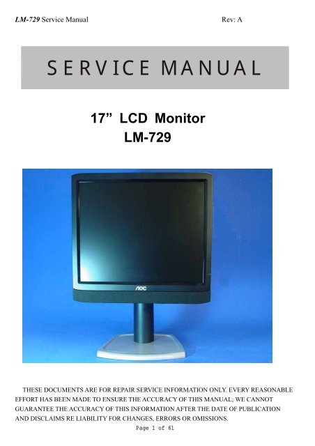
LM-729 <strong>Service</strong> ManualRev: ASERVICE MANUAL17” LCD MonitorLM-729THESE DOCUMENTS ARE FOR REPAIR SERVICE INFORMATION ONLY. EVERY REASONABLEEFFORT HAS BEEN MADE TO ENSURE THE ACCURACY OF THIS MANUAL; WE CANNOTGUARANTEE THE ACCURACY OF THIS INFORMATION AFTER THE DATE OF PUBLICATIONAND DISCLAIMS RE LIABILITY FOR CHANGES, ERRORS OR OMISSIONS.
LM-729 <strong>Service</strong> ManualRev: APrepared: ShiweiDate: Jul-30-03
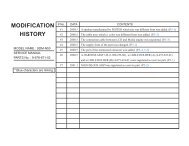
LM-729 <strong>Service</strong> ManualRev: ARevision HistoryRevision Date Page Items ModificationA Date:Jul-30-03 All First version release;
LM-729 <strong>Service</strong> ManualRev: ATable of ContentsTable of Contents ---------------------------------------------------------------------------------------------------31. MONITOR SPECIFICATIONS ---------------------------------------------------------------------------52. LCD MONITOR DESCRIPTION ---------------------------------------------------------------------------63. OPERATING INSTRUCTIONS ---------------------------------------------------------------------------73.1 GENERAL INSTRUCTIONS -------------------------------------------------------------------------73.2 CONTROL BUTTONS ------------------------------------------------------------------------------------73.3 ADJUSTING THE PICTURE--------------------------------------------------------------------------------74. Input/Output Specification - -------------------------------------------------------------------------------104.1 Input Signal Connector --------------------------------------------------------------------------------104.2 Factory Preset Display Modes -------------------------------------------------------------------------- 114.3 Power Supply Requirements ------------------------------------------------------------------------ 124.3.1 Input Requirements -------------------------------------------------------------------------------------124.3.2 Output Requirements ------------------------------ ------------------------------------------------124.4 PANEL SPECIFICATION -------------------------------------------------------------------------------144.4.1 Panel Feature ------------------------------------------------------------------------------------------144.4.2 Display Characteristics --------------------------------------------------------------------------------144.4.3 Optical Characteristics -------------------------------------------------------------------------------144.4.4 Parameter guide line for CCFL Inverter ------------------------------------------------------145. Block Diagram ------------------------------------------------------------- -----------------------------155.1 Monitor Exploded View ------------------------------------------------------------------------------------155.2 Software Flow Chart -------------------------------------------------------------------------------------165.3 Electrical Block Diagram ------------------------------------------------------------------------------185.3.1 Main Board -------------------------------------------------------------------------------------------------18
LM-729 <strong>Service</strong> ManualRev: A5.3.2 Inverter/Power Board -------------------------------------------------------------------------------------196. Schematic -------------------------------------------------------------------------------------------------------216.1 Main Board -----------------------------------------------------------------------------------------------216.2 AUDIO Board -----------------------------------------------------------------------------------------256.3 Key Board ------------------------------------------------------- ---------------------------------------266.4 Inverter/Power Board -----------------------------------------------------------------------------------277. PCB Layout -------------------------------------------------------------------------------------------------297.1 Main Board -----------------------------------------------------------------------------------------------297.2 Inverter/Power Board -----------------------------------------------------------------------------------317.3 Keypad Board And Audio board-------------------------------------------------------------------------348. Maintainability --------------------------------------------------------------------------------------------------348.1 Equipments and Tools Requirements ----------------------------------------------------------------358.2 Trouble Shooting ---------------------------------------------------------------------------------------------338.2.1 Main Board --------------------------------------------------------------------------------------------------358.2.2 Power/Inverter Board -------------------------------------------------------------------------- ----------388.2.3 Key Pad Board ---------------------------------------------------------------------------------------------409. White-Balance, Luminance adjustment ----------------------------------------------------------------4110. EDIT Content -------------------------------------------------------------------------------------------4211. BOM List -------------------------------------- -----------------------------------------------------------------43
LM-729 <strong>Service</strong> Manual1.MONITOR SPECIFICATIONSRev: ADriving systemTFT Color LCDLCD Panel Size 43.2cm(17.0")Pixel pitch 0.264mm( H )x 0.264mm( V )Viewable angleResponse time (typ.)Video90˚ (H) 90˚ (V)25 msAnalog /DigitalInput Sync. Type H/V TTLH-FrequencyV-Frequency30kHz – 80kHz55-75HzDisplay ColorsDot ClockOver 16 million Colors135MHzMax. Resolution 1280 x 1024Plug & PlayPower Consumption ON Mode
LM-729 <strong>Service</strong> ManualRev: A2. LCD MONITOR DESCRIPTIONThe LCD MONITOR will contain a main board, an inverter/power board, keypad board , Audio board andexternal power adapter which house the flat panel control logic, brightness control logic and DDC.The Inverter board will drive the backlight of panel and the DC-DC conversion.The Adapter will provide the 12V DC-power to inverter/power board.Monitor Block DiagramCCFT Drive.Flat Panel andCCFL backlightPower board(include:adapter,inverter)Main BoardKeyboardRS232 ConnectorFor white balanceadjustment infactory modeAC-IN100V-240VHOST ComputerVideo signal, DDC
LM-729 <strong>Service</strong> Manual3. OPERATING INSTRUCTIONS3.1 GENERAL INSTRUCTIONSRev: APress the power button to turn the monitor on or off. The other control buttons are located at front panel of the monitor. Bychanging these settings, the picture can be adjusted to your personal preferences.- The power cord should be connected.- Connect the video cable from the monitor to the video card.- Press the power button to turn on the monitor, the power indicator will light up.3.2 CONTROL BUTTONS- Power Button:When pressed, the monitor enters the off mode, and the LED turns blank. Press again to restore normal status.- Left / Right Button:When the OSD show on screen, Left/Right Button are used to control the monitor functions. Press to switch functions or adjustsettings. And if the OSD off, Left/Right buttons are used to control the audio volume;- Auto Adjust Key:The Auto Adjust Key is used to automatically set the H Position, V Position, Clock and Phase.- Power Indicator:Green — Power On mode.Orange — Power Saving mode.Blank —Power Off Mode.CONTROL ButtonsA B C D E FAuto Volume Menu LED PowerA. Menu buttonB. Left button/Volume downC. Right button/Volume upD. Auto button/ExitE. Indicator lightF. Power button3.3 ADJUSTING THE PICTURE
LM-729 <strong>Service</strong> ManualRev: AOSD Table:MainMenu ItemLuminanceImageSetupImagePositionColorTemp.AutoConfig(Analog-Only Model)Input Select(Dual-InputMainMenu IconSub MenuItemContrastSubMenuIconDescriptionAdjustRangeReset ValueContrast from Digital-register. 0-100 Recall CoolContrast ValueBrightness Backlight Adjustment 0-100 Recall CoolBrightness ValueFocusAdjust Picture Phase to reduce 0-100 Do Auto ConfigHorizontal-Line noiseClockAdjust picture Clock to reduce 0-100 Do Auto ConfigVertical-Line noise.H. Position Adjust the horizontal position 0-100 Do Auto Configof the picture.V. Position Adjust the verticalposition of 0-100 Do Auto Configthe picture.Warm N/A Recall Warm ColorN/A The ColorTemperature from EEPROM. Temperature willCool N/A Recall Cool ColorN/A be set to Cool.Temperature from EEPROM.User / RedRed Gain from0-100 The User R/G/BDigital-register.value(default isUser / Green Green Gain Digital-register. 0-100 100) will not beModified by ResetUser / BlueBlue Gain from0-100 function.Digital-register.Yes N/A Auto Adjust the H/V Position, N/A N/AFocus and Clock of picture.No N/A Do not execute Auto Config, N/A N/Areturn to main menu.Analog N/A Select input signal from analog N/A N/A(D-Sub)Model) Digital N/A Select input signal from digital N/A N/A(DVI)OSD SetupH. Position Adjust the horizontal position 0-100 50of the OSD.V. Position Adjust the verticalposition ofthe OSD.0-100 50OSD Timeout Adjust the OSD timeout. 10-120 10
LM-729 <strong>Service</strong> ManualRev: ALanguageEnglish N/A Set OSD display language to N/A The Language willEnglish.be set to English.Deutsch N/A Set OSD display language to N/AGerman.Français N/A Set OSD display language to N/AFrench.Español N/A Set OSD display language to N/ASpain.Italiano N/A Set OSD display language to N/AItalian.简 N/A Set OSD display language to N/ASimplified Chinese.Information Information N/A Show the resolution, H/V N/A N/Afrequency and input port ofcurrent iput timing.ResetYes N/A Clear each old status of N/A N/AAuto-configuration and set thecolor temperature to Cool.No N/A Do not execute reset, return to N/A N/Amain menu.Exit N/A N/A Exit OSD N/A N/A
LM-729 <strong>Service</strong> Manual4. Input/Output Specification4.1 Input Signal Connector4.1.1 Analog D-SUB ConnectorRev: APIN NO.DESCRIPTIONPI N NO.DESCRIPTION1. Red 9. +5V2. Green 10. Detect Cable3. Blue 11. NC4. Ground 12. DDC-Serial Data5. Ground 13. H-Sync6. R-Ground 14. V-Sync7. G-Ground 15. DDC-Serial Clock8. B-GroundVGA connector layout1 56 1011 154.1.2 DVI-D ConnectorDVI-D Connector to be compliant to the latest DVI-DDWG specification version available.Pin Meaning Pin Meaning Pin Meaning1TMDS Data2-9TMDS Data1-17TMDS Data0-2 TMDS Data2+ 10TMDS Data1+18TMDS Data0+3 TMDS Data 2/4Shield4not connected11 TMDS Data 1/3 Shield 19TMDS Data 0/5 Shield12 not connected 20 not connected5 not connected 13not connected21 not connected6 DDC Clock 14 +5V Power 22 TMDS Clock Shield7 DDC Data 15 Ground 23 TMDS Clock-8 Analogue VerticalSync16Hot Plug Detect24 TMDS Clock+
LM-729 <strong>Service</strong> ManualRev: A19174.2 Factory Preset Display ModesVESA MODESHorizontalVerticalNominal Sync Nominal Sync Nominal PixelMode Resolution Total Frequency Polarity Freq. Polarity Clock+/- 0.5kHz+/- 1 Hz(MHz)640x480@60Hz 800 x 525 31.469 N 59.940 N 25.175VGA 640x480@72Hz 832 x 520 37.861 N 72.809 N 31.500640x480@75Hz 840 x 500 37.500 N 75.00 N 31.500800x600@56Hz 1024 x 625 35.156 N/P 56.250 N/P 36.000SVGA800x600@60Hz 1056 x 628 37.879 P 60.317 P 40.000800x600@72Hz 1040 x 666 48.077 P 72.188 P 50.000800x600@75Hz 1056x625 46.875 P 75.000 P 49.5001024x768@60Hz 1344x806 48.363 N 60.004 N 65.0001024x768@60Hz 1312x813 48.78 N 60.00 N 64.000XGA1024x768@70Hz 1328x806 56.476 N 70.069 N 75.0001024x768@72Hz 1304x798 57.515 P 72.074 P 75.0001024x768@75Hz 1328x804 60.200 N 74.90 N 80.0001024x768@75Hz 1312x800 60.023 P 75.029 P 78.750XGA 1152x864@75Hz 1600x900 67.50 P 75.000 P 108.000SXGA1280x1024@60Hz 1688x1066 63.981 P 60.020 P 108.0001280x1024@75Hz 1688x1066 79.976 P 75.025 P 135.000IBM MODESHorizontalVerticalMode Resolution TotalNominalNominalNominalSyncSync PixelFrequencyFreq.PolarityPolarity Clock+/- 0.5kHz+/- 1 Hz(MHz)DOS* 720x400@70Hz 900 x 449 31.469 N 70.087 P 28.322DOS** 640x400@70Hz 800 x 449 31.469 N 70.087 P 25.175MAC MODESVGA 640x480@67Hz 864x525 35.000 N 66.667 N 30.240SVGA 832x624@75Hz 1152x667 49.725 N 74.551 N 57.2832
LM-729 <strong>Service</strong> Manual4.3 Power Supply Requirements4.3.1 Input RequirementsRev: APARAMETER RANGE CONDITIONInput AC Voltage 100 to 240VAC RMS Universal input full rangeInput Frequency 60Hz @ 100VAC to 50Hz @240VACInput Current Less than 2.0 Amps RMS Input voltage 100 VAC RMS ; 60 Hertz. Parametermust be reached within 3 seconds of turn-on. Less than 1.0 Amps RMS Input voltage 220 VAC RMS ; 50 Hertz. Parametermust be reached within 3 seconds of turn-on.Input Power Less than 75 Watts Power factor > 0.5 Input voltage 120 VAC RMS ; 60 HertzInrush Current Less than 30 A peak Input voltage 100 VAC RMS ; 60 Hertz at allPhase(0, 90, 180, 270 degree) Less than 50 A peak Input voltage 240 VAC RMS ; 50 Hertz at allPhase(0, 90, 180, 270 degree)Input Fusing Fuse should be located internal to the Fuse must be UL/CSA approved. Fuse value must noadapter, easily accessible when the have to change for 115 VAC or 230 VAC operationcover is removedLeakage Current Less than 3.5 mA Input voltage 240 Volts RMS ; 50 HertzHi-Pot Primary to secondary 1.5KVAC for 1 Minute(leakage current 10mA)1.8KVAC for 1 Minute(leakage current 10mA)3.0KVAC for 1 Minute(leakage current 10mA)without Y-cap & Coupling cap. Prima1ry to Safety Ground 1.5KVAC for 1 Minute(leakage current 10mA)1.8KVAC for 1 Minute(leakage current 10mA)4.3.2 Output RequirementsPARAMETER RANGE CONDITIONDC Out 12VDC ± 5% Min 0A Max 3.75ALoad Regulation 12.0V(12.12V) ± 5% 11.4 to 12.6VDCDynamic Load Any frequency up to 250Hz(duty5% for 10% to 100%, 100% to 10% load change forRegulation 50%)+12VdcRipple & noise 170mVpp at 12VDC Input voltage : 100VAC at 60Hz 240VAC at 50Hz* Ripple and noise are measured.Output current less than 7.0A, more than 12.0A Current exceeds maximum rateing more than 20%protection at 12.0VDCLeakage Current Less than 0.25 mA Input voltage 100 Volts RMS ; 50 Hertz Less than 0.5 mA Input voltage 240 Volts RMS ; 50 Hertz
LM-729 <strong>Service</strong> Manual4.4 PANEL SPECIFICATION4.4.1 Panel Feature-High contrast ratio, high aperture structure-TN(Twisted Nematic) mode-Wide viewing angle-High speed response-SXGA(1280 x 1024 pixels) resolution-Low power consumption-2 dual CCFTs(Cold Cathode Fluorescent Tube)-DE(Data Enable) mode-COMPACT SIZE DESIGNRev: A4.4.2 Display CharacteristicsItems Specification UnitDisplay Area 337.92(H) x 270.336(V) mmDriver elementa-Si TFT active matrixDisplay color 16.2M ColorsNumber of pixels 1280 x 1024 pixelPixel ArrangementRGB vertical stripePixel pitch 0.264(H) x 0.264(W) mmDisplay ModeNormally White4.4.3 Optical CharacteristicsThe optical characteristics are measured under stable conditions at 25 (Room Temperature):Item Symbol Conditions Min. Typ. Max. Unit NoteContrast Ratio(Center of screen) 250 450 -Response Rising Tr - 4 5Time Falling Tf - 12 20msecLuminance of WhiteNormalYL(Center of screen)=0200 260 - Cd/m2Rx =00.64Ry Viewing0.34ColorGx 0.29ChromaticityTyp.TYP.Gy 0.61(CIE 1931)-0.03+0.03Bx 0.14Coordinates (CIE)By 0.07Wx 0.31Wy0.33Brightness Uniformity [%] 75 80 -
LM-729 <strong>Service</strong> ManualRev: A4.4.4 Parameter guide line for CCFL InverterINVERTER MAX BRINGTHNESS (Vadj:5.0v), LOAD=120KX4(ROOM TEMPERATURE 25 4)ITEM SYMBOL MIN. TYP. MAX. UNIT REMARKInput voltage Vin 10.8 12 13.2 VInput current Iin 2250 2500 mA FOR 4 LOADOutput Current Iout 6.0 6.5 7.0 mA FOR 1 LOADFrequencyF 50.0 55.0 60.0 KHZFOR 1 LOADH.V open Vopen 1450 1600 1750 Vrms NO LOADH.V Load Vload 710 810 910 Vrms RL=120KStart voltage Vst 1650 1750 1850 Vrms RL=CCFLProtect delay time PDT 0.4 1 4 SecINVERTER MIN BRINGTHNESS (Vadj:0.0v), LOAD=120KX4(ROOM TEMPERATURE 25 4)ITEM SYMBOL MIN. TYP. MAX. UNIT REMARKinput voltage Vin 10.8 12 13.2 Vinput current Iin 660 750 mA FOR 4 LOADOutput Current Iout 3.0 3.5 4.0 mA FOR 1 LOADFrequencyF 50.0 55.0 60.0 KHZFOR 1 LOADH.V open Vopen 1450 1600 1750 Vrms NO LOADStart voltageVst1650 1750 1850 Vrms RL=CCFLH.V Load Vload 350 450 550 Vrms RL=120K
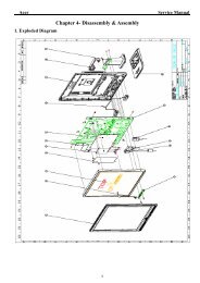
LM-729 <strong>Service</strong> Manual5. Block Diagram5.1 Monitor Exploded ViewRev: A
LM-729 <strong>Service</strong> Manual5.2 Software Flow ChartRev: A12NY345NY67YN8910N11YN1213NYY1415N16Y1718N19Y
LM-729 <strong>Service</strong> ManualRev: ARemark:1) MCU initialize.2) Is the EEprom blank ?3) Program the EEprom by default values.4) Get the PWM value of brightness from EEprom.5) Is the power key pressed ?6) Clear all global flags.7) Are the AUTO and SELECT keys pressed ?8) Enter factory mode.9) Save the power key status into EEprom.Turn on the LED and set it to green color.Scalar initialize.10) In standby mode ?11) Update the life time of back light.12) Check the analog port, are there any signals coming ?13) Does the scalar send out a interrupt request ?14) Wake up the scalar.15) Are there any signals coming from analog port ?16) Display "No connection Check Signal Cable" message. And go into standby mode afterthe message disappear.17) Program the scalar to be able to show the coming mode.18) Process the OSD display.19) Read the keyboard. Is the power key pressed ?
LM-729 <strong>Service</strong> Manual5.3 Electrical Block Diagram5.3.1 Main BoardRev: ALCDInterface(CN4/CN5)Flash MemoryW39f010P-70B(U6)Scalar gm5126/gm2126(Include MCU,ADC,OSD)(U4)OSDControlInterface(CN9)EPR_SDAEPR_SCLEEPROM24C16(U7)RGBRXDTXDD-SubConnector(CN2)Hsync,VsyncDVI-I onlyConnector(CN1)DB15_SDA,DB15_SCLEEPROM24C02(U2)EEPROM (D-I only)24C02(U1)
LM-729 <strong>Service</strong> Manual5.3.2 Inverter/Power BoardRev: AInverter Block DiagramVinBuck ConnectorParallet-resonantinverterDriverCircuitDimming control(PW M )( )VinParallet-resonantinverterCCFLDriverCircuitDimming controlPWM
LM-729 <strong>Service</strong> Manual Rev: APower Block DiagramPWPC7425A3
21LM-729 <strong>Service</strong> Manual Rev: A+3V3+3V3+3V33V3_DDDSFB18FB5FB4600 OHM+ 600 OHM600 OHMC23C24C2522uF/16V0.1uF/16V0.1uF/16VC27 C28 C29GNDGNDGND3V3_SDDSFB6+3V3GNDClose to respective power Pins+2V50.1uF/16VC33 C34 C31 C32C30FB19600 OHM GND Close to respective power Pins0.1uF/16V0.1uF/16V0.1uF/16VR5310K 1/16WR49NCNC+5VR220R221R222R67R60R61R62R63NC NC NC+3V3NCBOOTSTRAP SIGNALSADDRESSNAME SETROM_ADDR(4:0) USER_BITS(4:0) xROM_ADDR5 ReservedxROM_ADDR6 SCLPOLxROM_ADDR7 HOST_PROTOCOL 0ROM_ADDR8 HOST_PORT_EN 1ROM_ADDR9 OCM_START 1ROM_ADDR(12:10) USER_BITS(7:5) xROM_ADDR13 OSC_SEL0ROM_ADDR14 OCM_ROM_CFG(1) 1NCR500 1/16WNCNC+PV+PVR6410K 1/16WR6510K 1/16W+3V3R464.7K 1/16W1 = All 48K of ROM is in external ROM3R66+ C7022uF/16VU5 TCM809SENB713/NCVCCGNDRSTRMADDR14RMADDR9RMADDR8RMADDR10RMADDR11RMADDR3RMADDR4RMADDR12RMADDR2RMADDR1RMADDR0R5610K 1/16W +PVDESCRIPTIONAvailable for reading from a status registerIf using 6-wire host protocol, program this bit to 0Determines polarity of HCLK signal+3V3ROM_WEBANK010K 1/16W2+3V3C4822uF/16VIf using 6-wire host protocol, program this bit to 1GPIO(22:16) is on "Host Port" pinsGNDAvailable for reading from a status register+GND+3V3D14LL41481 = OCM becomes active after OCM_CLK is stable0 = XTAL and TCLK pins are connected1BANK1ResetCircuitR48NCFB7600 OHMC4922uF/16VDIGITAL PORTROMCEFB8600 OHM+PVR5710K 1/16WR590 1/16WRMADDR15RMADDR14RMADDR13RMADDR12RMADDR11RMADDR10RMADDR9RMADDR8RMADDR7RMADDR6RMADDR5RMADDR4RMADDR3RMADDR2RMADDR1RMADDR0R2190 1/16W4772422222222222222222222+GNDC5722uF/16VSTDBYVGA_PGCTRLP12VDDC_SDA_ADDC_SCL_AR218NCGND+DDC_SCL_DDDC_SDA_DC50 C510.1uF/16V 0.1uF/16VPPWRPBIASRED+RED-GREEN+GREEN-BLUE+BLUE-HSVSGNDC580.1uF/16V+2V5ROMCEBANK1C520.1uF/16VC590.1uF/16V+3V3FB9C685pF/50VC695pF/50V3V3_RGBC530.1uF/16V3V3_DVI600 OHMC600.1uF/16VC6422uF/16VC54 C550.1uF/16V 0.1uF/16VGND+ C650.1uF/16VC66 NCR47X1NC14.318MHzR223 0 1/16WR224 NCR217RESETU631WE302NC/A173A1629A1521 RMDATA728A14 DQ720 RMDATA64A13 DQ619 RMDATA525A12 DQ518 RMDATA423A11 DQ417 RMDATA326A10 DQ315 RMDATA227A9 DQ214 RMDATA15A8 DQ113 RMDATA06A7 DQ0+PV7A68A59A410A311A212A11A0 NCFB10600 OHM243222OE VCC16CE GNDC710.1uF/16VW39F010PR22510K 1/16WGND32-Pin PLCC SocketFLASH/ Prom-Jet Socket600 OHMC610.1uF/16VNCC3522uF/16VAGND+3V3C620.1uF/16VGND+GNDGNDXTALTCLKRMADDR15RMADDR14RMADDR13RMADDR12RMADDR11RMADDR10RMADDR9RMADDR8RMDATA6RMDATA5RMDATA4RMDATA3RMDATA2RMDATA1RMDATA0ROM_OEnC67NCGNDBANK0C370.1uF/16VAGND153149145141156155152148144135132126120112136129123117114138172168163137787917517490919293898810810910781150151146147142143176177154133134118119124125130131R51 1K 1/16W113RMADDR7RMADDR6RMADDR5RMADDR4RMADDR3RMADDR2RMADDR1RMADDR0AGNDROM_WE180181182183184187188189190191192193194195196197200201202203204205206207208TCLKXTALU4GM5126AVDD_ADCAVDD_REDAVDD_GREENAVDD_BLUESGND_ADCAGND_ADCAGND_REDAGND_GREENAGND_BLUEAVDD_RXCAVDD_RX0AVDD_RX1AVDD_RX2AVDD_IMBAGND_RXCAGND_RX0AGND_RX1AGND_RX2AGND_IMBAVSS_RPLLAVSS_DDDSAVSS_SDDSGND_RXPLLPPWRPBIASRXC+RXC-RX2+RX2-RX1+RX1-RX0+RX0-RED+RED-GREEN+GREEN-BLUE+BLUE-HSYNCVSYNCADC_TESTRXC+RXC-RX2+RX2-RX1+RX1-RX0+RX0-REXT173VDD_RXPLL_2.5GPIO20/HDATA3GPIO19/HDATA2GPIO18/HDATA1GPIO17/HDATA0GPIO16/HFSGPIO22/HCLKGPIO14/DDC_SCLGPIO15/DDC_SDARESETnGPIO11/ROM_WEnROM_ADDR15ROM_ADDR14ROM_ADDR13ROM_ADDR12ROM_ADDR11ROM_ADDR10ROM_ADDR9ROM_ADDR8ROM_ADDR7ROM_ADDR6ROM_ADDR5ROM_ADDR4ROM_ADDR3ROM_ADDR2ROM_ADDR1ROM_ADDR0ROM_DATA7ROM_DATA6ROM_DATA5ROM_DATA4ROM_DATA3ROM_DATA2ROM_DATA1ROM_DATA0ROM_OEnAVDD_RPLL162164VDD_SDDSAVDD_SDDS167169VDD_DDDSAVDD_DDDSRVSSRVSSRVSSRVSSEAVSS_RSEAVSS_RSAVSS_RSOAVSS_RSOAVSS_RS771021791991426384860GND17176101178198VDD_DPLLRVDDRVDDRVDDRVDDCVSSCVSSCVSSCVSS368511118611512112715816013253747593584110185VDD_RX2_2.5VDD_RX1_2.5VDD_RX0_2.5VDD1_ADC_2.5VDD2_ADC_2.5EAVDD_RS_2.5EAVDD_RS_2.5AVDD_RSOAVDD_RS_2.5OAVDD_RS_2.5CVDD_2.5CVDD_2.5CVDD_2.5CVDD_2.5157159116122128GPIO10/TCON_ROE3GPIO9/TCON_ROE2GPIO21/TCON_FSYNCGND1_ADCGND2_ADCGND_RX2GND_RX1GND_RX0VSS_DPLLVSS_DDDSVSS_SDDSGPIO12/NVRAM_SDAGPIO13/NVRAM_SCLGPIO8/IRQINnGPIO0/PWM0GPIO1/PWM1GPIO2/PWM2GPIO3/TIMER1GPIO6/TCON_SHCGPIO7/TCON_TDIVGPIO4/UART_DIGPIO5/UART_DO170166161OCH11P_RSOCH11N_RSOCH10P_RSOCH10N_RSOCH9P_RSOCH9N_RSOCH8P_RSOCH8N_RSOCH7P_RSOCH7N_RSOCH6P_RSOCH6N_RSOCH5P_RSOCH5N_RSOCH4P_RSOCH4N_RSOCLKP_RSOCLKN_RSOCH3P_RSOCH3N_RSOCH2P_RSOCH2N_RSOCH1P_RSOCH1N_RSOCH0P_RSOCH0N_RSECH11P_RSECH11N_RSECH10P_RSECH10N_RSECH9P_RSECH9N_RSECH8P_RSECH8N_RSECH7P_RSECH7N_RSECH6P_RSECH6N_RSECH5P_RSECH5N_RSECH4P_RSECH4N_RSECLKP_RSECLKN_RSECH3P_RSECH3N_RSECH2P_RSECH2N_RSECH1P_RSECH1N_RSECH0P_RSECH0N_RSTCON_OSPTCON_OPOLTCON_OINVTCON_RSP2TCON_RSP3TCON_RCLKTCON_ROETCON_ESPTCON_EINVTCON_EPOLDHS/TCON_LPReservedReservedN/CN/CCLKOUT6867666564636261585756555453525150494645444342414039343332313029282724232221201918171615121110987656971707273747512348010510682839495969798103104991008687139165140+C3622uF/16VGNDSDASCLGPIO2GPIO3GPIO6GPIO7GNDC47GPIO0/PWM00.1uF/16VC38OD22POD22NOD21POD21NOD20POD20NOD12POD12NOD11POD11NOD10POD10NOCLK_RS_POCLK_RS_NOD02POD02NOD01POD01NOD00POD00NED22PED22NED21PED21NED20PED20NED12PED12NED11PED11NED10PED10NECLK_RS_PECLK_RS_NED02PED02NED01PED01NED00PED00N10K 1/16W0.1uF/16V+3V3R70SCLSDA10K 1/16WC39R87 33 1/16WR88 33 1/16WR89 33 1/16WR92 33 1/16WR52 22 1/16WR54 22 1/16WR55 22 1/16WDVI_PLUGR68NC+5VR710.1uF/16VGNDTitleC400.1uF/16VADD DEN SIGNAL PIN 4/28OD22P 4OD22N 4OD21P 4OD21N 4OD20P 4OD20N 4OD12P 4OD12N 4OD11P 4OD11N 4OD10P 4OD10N 4OD02P 4OD02N 4OD01P 4OD01N 4OD00P 4OD00N 4ED22P 4ED22N 4ED21P 4ED21N 4ED20P 4ED20N 4ED12P 4ED12N 4ED11P 4ED11N 4ED10P 4ED10N 4ECLK_RS_P 4ECLK_RS_N 4ED02P 4ED02N 4ED01P 4ED01N 4ED00P 4ED00N 4R690 1/16W<strong>AOC</strong>TCON_OSPTCON_RSP2TCON_RCLKTCON_ROETCON_ESPTCON_EPOLTCON_LPLED_ORANGE 5LED_GRN 5DVI_PLUG 2GPIO8 5PWM0 7VOLUME 7GPIO2 5GPIO3 5GPIO6 5GPIO7 5GPIO4UART_DI 2GPIO5UART_DO 2C720.1uF/16VU7gm5126C41OCLK_RS_P 4OCLK_RS_N 48765VCCWPSCKSI0.1uF/16VA0A1A2VSSM24C16-MN6TC4212340.1uF/16VC430.1uF/16VTCON_OSP 4TCON_RSP2 4TCON_RCLK 4TCON_ROE 4TCON_ESP 4TCON_EPOL 4TCON_LP 4GNDC440.1uF/16VC79 GND22pF/NCGNDC45C7422pF/NC0.1uF/16VC46GNDC8622pF/NCGND0.1uF/16VC7622pF/NCSize Document Number RevC gm5126ADate: , 22, 2003Sheet of 3 8
LM-729 <strong>Service</strong> Manual Rev: AED01P3OD22N+12VED10N3R8410KPPWR3TCON_OSP3OD20NOD22PR79NCGNDED20P3ED00N3ED22POD01N3GNDED20N3ECLK_RS_NOD11N+C75100uF/16VGNDTCON_LPGNDTCON_ROE3R202 NCED12NR853K 1/16WOCLK_RS_P3OD12NR76 0 1/16WECLK_RS_N3+C78150uF/16VOD21N3GNDOD10N3TCON_ESPOCLK_RS_N3OD22N3ED12PR74 NCGNDED20P+P3V3OD10PTCON_RSP23ED10P3OD02NR82100K 1/16W+P5VED02P3+C73100uF/16VOD22P3ED20NED11POD01POD00N3ED21N3GNDTCON_RCLKED01POD21NCONNECTOR for PANELFB11NCGNDED10NTCON_LP3OCLK_RS_PED10P+P5VOD02N3ED12N3ED00PCN4CONNECTOR 50P1234567891011121314151617181920212223242526272829303132333435363738394041424344454647484950OD02P3C77100pFED00P3R730 1/16WED11P3R201510K 1/16WOD12P3+P3V3OD00PCN5CONNECTOR 30P123456789101112131415161718192021222324252627282930PPWR3TCON_RSP2C820.1uF/16VOD10N+3V3OD20P3R863K 1/16WR77NCTCON_EPOL3GNDOD12N3R720 1/16WED00NECLK_RS_P3ED22P3+5VED01NOD20POD11N3TCON_ROEFB12220 OHMR80100K 1/16WGNDED01N3ED02PED21PR81 NCOD02PED22N3OCLK_RS_N+12VGNDED22NQ5PMBS3904321TCON_ESP3ED21P3ED21NOD21PED12P3OD11P3ED11N3R78NCgm5126APanel Interface(RSDS)<strong>AOC</strong>B4 8, 22, 2003TitleSize Document Number RevDate: Sheet ofOD20N3ECLK_RS_POD00NQ1PMBS3904321GND+C20022uF/16VOD11PTCON_EPOLQ2SI9933ADY-T112348765S1G1S2G2D1D1D2D2R750 1/16WGNDR203100K 1/16W+C205150uF/16VCTRLP12V3R83 NCTCON_RCLK3ED02NOD00P3GNDOD01NED02N3OD12PR200100K 1/16WOD01P3ED11NC800.1uF/16V+12VOD10P3OD21P3
LM-729 <strong>Service</strong> Manual Rev: A+3V3+5V3U8VIN VOUT2CN6016P PLUG R/AC1250.1uF/16VGND1ADJAIC1084-33CER1161K 1/16W R1181.5K 1/16WC1240.1uF/16VGND+ C126100uF/16V3VOLUMEFB15600 OHMFB16600 OHM123456R232Standby 10K 1/16W+C2311uF/16VGNDGNDD20 LL4148R23110K 1/16WSTDBY 3FB17GND 600 OHM MuteR230 10K 1/16WD21+12V+5V+12V+5V+ C2301uF/16VLL4148+5VC111 + C110100uF/16V 0.1uF/16VGND31U9VIN VOUTADJAIC1084-33CE2R1121K 1/16WR1141K 1/16WC1190.1uF/16V+2V5+ C120100uF/16VGND3PBIASR1134.7KC117100uF/16V+5V+ C1210.1uF/16VBackLightOn/Off24681012GNDCN111357911PIN HEADER 2*6PGNDCONNECTOR forPOWER/INVERTERBoardGNDGNDGNDR1154.7KPWM0PWM0BrightnessBrightnessR1171K+ C12722uF/16VGND<strong>AOC</strong>TitlePowerSize Document Number RevB gm5126ADate: , 22, 2003Sheet of 7 8
LM-729 <strong>Service</strong> Manual Rev: A6.2 AUDIO BoardOUT_LOUT_RCN202WAFER 2*7P 2.54mm+12V12VMUTEFB200BEAD1311975311412108642+C201470uF/16V+C202470uF/16VC2030.1uFC2151000 pFC214CN20412333L8022-3A-H FEMALEGNDR201 10K 1/4WR203 10K 1/4WC211100 pFR2105.6K 1/4WR2115.6K 1/4WVOLUMEC212100 pFR212220K 1/4W+ C2091.0uFGNDC204C206+ C2101.0uFSTANDBY0.47uF0.47uFC2130.1uF4961112INLINR8VOLUMESTBYMUTENC16GNDGNDGND123VS15VSU201VAROUT_RVAROUT_LGNDGNDGNDGND13181920OUTLOUTRSVRTDA7496L!17141075C208470uF/16V+R2071K 1/4WGNDC205+470uF/16V+C207470uF/16VR2081K 1/4WGND1000 pF4321CN203WAFER 4P2.0 R/AGNDGNDGNDGNDTitleTitleSize Document Number RevA AudioSize Document Date: Number , 21, 2003Sheet 1 of Rev 1A Date: , 21, 2003Sheet 1 of 1
LM-729 <strong>Service</strong> Manual Rev: A6.3 Key Board14U3E3LED_ORANGE11 1074LCX1414U3F3LED_GRN13 1274LCX1477R900 1/16WR910 1/16W 3SOT-23C12BELED_GRNLED_ORG+3V3CN9LED_GRNKEY_AUTOKEY_RIGHTKEY_ONOFF13572468LED_ORGKEY_MENUKEY_LEFTR9410K 1/16WRP210K 1/16W8765C830.001uF1234C840.001uFC850.001uFC880.001uFWAFER 8P2.0 DUAL R/AC960.001uFC970.001uFC980.001uF33333GPIO6GPIO8GPIO3GPIO7GPIO21234RP387654.7K 1/16WR95 4.7K 1/16WKEY_LEFTKEY_AUTOKEY_MENUKEY_RIGHTKEY_ONOFFGNDGND<strong>AOC</strong>TitleKeypadSize Document Number RevB gm5126ADate: , 22, 2003Sheet of 5 8
32132412724LM-729 <strong>Service</strong> Manual Rev: A6.4 Inverter/Power BoardR92047 1/2WC9200.001uF/500V1- +DB9012KBP06M32 3L9021 4C904 0.47uF/250VD9041N4148+ C905120uF/400VC9080.1uFR9061M 1/4WR9071M 1/4WR9041M 1/4WR9051M 1/4W+C90710uFC9060.0015uF/2KVD902PS102RT9011O 9R903100K 2WO 7,8D901UF40073 7,85R90810 1/4W 10,114OD910R922 C92147 1/4W 0.001uF/500VD912++L903C9221000uF/16VL904C9251000uF/16V+C924470uF/16V+C926470uF/16VF9020 1/16WFB9030 1/16WZD904SML4736FB902C9280.1uFCON10212 12V11 GND109876 GND5 GND4 5V3 5V2 DIM1 ON/OFFR9011M 1/16W22 31 4C9031L9010.1uF/250VR9021M 1/16WC901 C9020.001uF/250V 0.001uF/250VtF901FUSENR901NTCRD9051N4148P901A12Wire HarnessIC901SG6841R91624K 1/10WR9094.7K 1/16WZD901RLZ20BR913N.C_0603R912100 1/16W1 34SG68415 6C912N.CR91510K 1/16WC9110.001uFR914N.C/06038C9090.1uFR917JUMPER21R91820K 1/4WR9104.7K 1/16WQ9012PA733PQ9022PC945PC910 R9110.1uF4.7K 1/16WQ9032SK2996FB901BEADR9190.39 2WD9031N4148C913R9300.0022uF/250V100 1/4WZD902HZ12B2IC902PC123FY2 4PC9360.1uFIC903HTL431R9311K 1/16WR929JUMPERC9350.01uFZD903HZ5C1R9271K 1/4WR9281K 1/4WR92433K 1/4WR9262.4K 1/4WR9253.6K 1/4WC9270.1uFCN901Size Document Number RevB PWPC7425B31Date: Sheet of 1 2
332212345673322LM-729 <strong>Service</strong> Manual Rev: A+12V++C201 C223150uF/25V 150uF/25VC2020.1uF/25VQ202DTA144WKAC2251uF/25VR2143.9K 1/16WR2123.9KQ203 SI4431DY-T118273645D201SR24L201D203RLZ11BR2242KR2252KR2262K 1/16WR2272K 1/16WPT2015 9C21522pF/3KVC21622pF/3KV1234CN202NO/OFFDIMR20130KC2031uF/25VR20210KQ201DTC144WKAR2084.7K 1/16W R21015KR21847013 2Q205MPS3904Q207MPS3906R216220 1/16WC2111uF/25VR22015KR22212KQ2092SC57061C2130.22uF/100VQ2102SC570613,4261 7POWER X'FMRR2321KD2091N4148D2051N4148R20547KC2091uF/25VR24051KD2071N4148R234910 1/4WC2050.1uFC2210.47uF/63VR23812KC2191uF/25VR236620+C20710uFR207OPENC2060.1uFR20647KCT REF16RT SCP151IN+ 2IN+141IN- 2IN-131FBK 2FBK121DTC 2DTC111OUT 2OUT108GND Vcc9C2040.1uFU201TL1451ACNSRC2241uF/25VR2153.9K 1/16WR2133.9KQ204 SI4431DY-T118273645D202SR24L202D204RLZ11BR2282KR2292KR2302KR2312KPT2025 9C21722pF/3KVC21822pF/3KV1234CN201C208330pFR20310KR20410KC2101uF/25VR2094.7K 1/16WR21115KR21947013 2Q206MPS3904Q208MPS3906R217220 1/16WC2121uF/25VR22115KR22312KQ2112SC57061C2140.22uF/100VQ2122SC570613,4261 7POWER X'FMRR2331KD2101N4148D2061N4148R24151KD2081N4148R235910 1/4W<strong>AOC</strong> (Top Victory) Electronics Co., Ltd.Titleis power GNDC2220.47uF/63VR23912KC2201uF/25VR237620Size Document Number RevBAis signal GNDFriday, July 25, 2003Date: Sheet of 2 2
LM-729 <strong>Service</strong> Manual Rev: A7. PCB Layout7.1 Main Board
LM-729 <strong>Service</strong> Manual Rev: A
LM-729 <strong>Service</strong> Manual Rev: A7.2 Inverter/Power Board
LM-729 <strong>Service</strong> Manual Rev: A7.3 Keypad Board and Audio board1. Keypad Board
LM-729 <strong>Service</strong> Manual Rev: A2.Audio Board
LM-729 <strong>Service</strong> Manual Rev: A8. Maintainability8.1 Equipments and Tools Requirement1.) Voltmeter.2.) Oscilloscope.1.) Pattern Generator.2.) DDC Tool with a IBM Compatible Computer.3.) Alignment Tool.4.) LCD Color Analyzer.5.) <strong>Service</strong> Manual.6.) User Manual.
LM-729 <strong>Service</strong> Manual Rev: A8.2 Trouble Shooting8.2.1 Main Board1.NO SCREEN APPEARMeasured CN11 pin5 = 12 V?Measured CN11 pin 9/10= 5V?Measured U8 pin 2= 3.3V?Measured U9 pin 2= 2.5V?Yes, all DC level existDisconnected the Signal cable( Loose theSignal cable ),Is the screen show “Cable NotConnected” ?Check Correspondent component.Is there any shortage or cold solder?Yes. there have OSD showConnected the Signal cable again,Check LED status.Led GreenLed OrangeNo, nothing is showConnected the Signal cable again,Check LED status.Check Power switch is in Power-onstatus , and check if Power switch hadbeen stuck ?Led orangeReplace U6Flash RomLed GreenOK, Keyboard no stuckCheck the Wire-Harness from CN2OK,Wire tight enoughMeasured RGB (R15,R17,R24) H,V Input atU4 pin 176,177 ,was there have signal ?Check digital signal from CN1NGCheck Correspondentcomponent short/open( Protection Diode )Check Panel-Power Circuit BlockOK,Panel Power OKOK,input NormalCheck U4 Data-output BlockMeasured Crystal X1(14.318MHz)OK, U4 data OKOK,clockReplace Power board and CheckInverter control relative circuitReplace U203 (GM5126/2126)Re-do White balance adjustOKNote: 1. if Replace “MAIN-BOARD” , Please re-do “DDC-content” programmed & “WHITE-Balance”.2. if Replace “Power Board” only, Please re-do “ WHITE-Balance”
LM-729 <strong>Service</strong> Manual Rev: A2.PANEL-POWER CIRCUITcheck R203 should have response from 0V to 5VWhen we switch the power switch from on to offNGCheck the PPWR panel power relative circuit,Q5, Q2(pin7,8)In normal operation, when LED =green, R203should =0 v,OK, R86 have responseNG, no VoltageMeasured the Q302 pin 7,8= 5 V?OKReplace Q302 ( N-MOS, SI993OK3.INVERTER Control Relative CircuitMeasured the inverter connector CN11pin 2 on/off control=5V (on)pin4 PWM signal control dim 0V-5VNG, still no screenNG Check the Bklt-On relative circuit, R113, R115, R117,In normal operation, when LED =green,R405 Bklt-On should =5 v,If Bklt-On no-response when the power switch turn on-off,Replace U4 GM5126/2126Replace Power board to new-one, andNGReplace Power board& Re-do white balanceCheck the screen is normal ??OK
LM-729 <strong>Service</strong> Manual Rev: A4.U4-DATA OUTPUTMeasured DCLK(pin 15 or pin 16 from U4)DVS, DHS (pin 1,4 from U4 )Is the waveform ok?DCLK around 48 MHZ , DVS=60.09Hz , DHSaround 80 KHz ?(refer to inputsignal=640x480@60 Hz 31k, and LED isGreen)NG , no transitionReplace GM5126 /2126 (U4) orreplace MAINBOARD.OKCheck U4 GM5126/2126Signal output(PIN17-22,27-32,39-44,51-56,61-66)Is the waveform ok ?If MainBoard being replace , pleasedo the DDC – content reprogrammedOKOK
LM-729 <strong>Service</strong> Manual Rev: A8.2.2 Power/Inverter Board1.) No powerNGOKOKNGOKNGNGRepeating the start voltageNGOK
LM-729 <strong>Service</strong> Manual Rev: A2.) W / LED , No BacklightOKNG OKNGOKNGOKNGOKNGOKNGCheck Q209/Q210/C213 orQ211/Q212/C214NGOK
LM-729 <strong>Service</strong> Manual Rev: A8.2.3 KeyPad BoardOSD is unstable or not workingIs KeyPad Board connecting normally ?YIs Button Switch normally ?YIs KeyPad Board Normally ?YNNNConnect KeyPad BoardReplace Button SwitchReplace KeyPad BoardCheck Main Board
LM-729 <strong>Service</strong> Manual Rev: A9. White-Balance, Luminance adjustmentApproximately 30 minutes should be allowed for warm up before proceeding white balance adjustment.Before started adjust white balance ,please setting the Chroma-7120 MEM. channel 1 to 6500 color, MEM. channel 2 to7800 color, ( our 6500 parameter is x = 313 10, y = 329 10, Y = 200 10 cd/m 2 ,7800 parameter is x = 296 10, y = 311 10, Y = 200 10 cd/m 2 )How to setting MEM.channel you can reference to chroma 7120 user guide or simple use “ SC” key and “ NEXT” key tomodify xyY value and use “ID” key to modify the TEXT descriptionFollowing is the procedure to do white-balance adjustPress MENU button during 2 seconds along with plug Power core will activate the factory mode, then MCU will doAUTO LEVEL automatically. Meanwhile press MENU the OSD screen will located at left top of panel.I. Bias adjustment :1. set the contrast to 70.2. adjust the Brightness to 90.II. Gain adjustment :Move cursor to “-Factory-” and press MENU keya. adjust 6500 color-temperature1 Switch the chroma-7120 to RGB-mode (with press “MODE” button )2 switch the MEM.channel to Channel 01 ( with up or down arrow on chroma 7120 )3 The lcd-indicator on chroma 7120 will show x = 313 , y = 329 , Y = 200 cd/m 24 Adjust the RED on OSD window until chroma 7120 indicator reached the value R=1005 adjust the GREEN on OSD, until chroma 7120 indicator reached G=1006 adjust the BLUE on OSD, until chroma 7120 indicator reached B=1007 repeat above procedure ( item 4,5,6) until chroma 7120 RGB value meet the tolence =1008 Press Exit on OSD window to save the adjustment resultb. adjust 7800 color-temperature9 Switch the chroma-7120 to RGB-mode (with press “MODE” button )10 switch the MEM.channel to Channel 02 ( with up or down arrow on chroma 7120 )11 The lcd-indicator on chroma 7120 will show x = 296 , y = 311 , Y = 200 cd/m 212 Adjust the RED on OSD window until chroma 7120 indicator reached the value R=10013 adjust the GREEN on OSD, until chroma 7120 indicator reached G=10014 adjust the BLUE on OSD, until chroma 7120 indicator reached B=10015 repeat above procedure ( item 12,13,14) until chroma 7120 RGB value meet the tolence =10016 Press Exit on OSD window to save the adjustment resultTurn the POWER-button off to on to quit from factory mode.
LM-729 <strong>Service</strong> Manual Rev: A10. EDIT ContentA. D-SUB Connector (Analog) Note: Byte 0C, 0D, 0E, 0F means Serial No. Byte 10, 11 means Manufacture Time. Byte 7F means checksumB. DVI Connector (Digital) Note: Byte 0C, 0D, 0E, 0F means Serial No. Byte 10, 11 means Manufacture Time. Byte 7F means checksum
LM-729 <strong>Service</strong> Manual Rev: A11. BOM List
LM-729 <strong>Service</strong> Manual Rev: A
LM-729 <strong>Service</strong> Manual Rev: A
LM-729 <strong>Service</strong> Manual Rev: A
LM-729 <strong>Service</strong> Manual Rev: A
LM-729 <strong>Service</strong> Manual Rev: A
LM-729 <strong>Service</strong> Manual Rev: A
LM-729 <strong>Service</strong> Manual Rev: A
LM-729 <strong>Service</strong> Manual Rev: A
LM-729 <strong>Service</strong> Manual Rev: A
LM-729 <strong>Service</strong> Manual Rev: A
LM-729 <strong>Service</strong> Manual Rev: A
LM-729 <strong>Service</strong> Manual Rev: A
LM-729 <strong>Service</strong> Manual Rev: A
LM-729 <strong>Service</strong> Manual Rev: A
LM-729 <strong>Service</strong> Manual Rev: A
LM-729 <strong>Service</strong> Manual Rev: A