HL 50 Poster II - DPG-Verhandlungen
HL 50 Poster II - DPG-Verhandlungen
HL 50 Poster II - DPG-Verhandlungen
You also want an ePaper? Increase the reach of your titles
YUMPU automatically turns print PDFs into web optimized ePapers that Google loves.
Semiconductor Physics Thursday<br />
conductive compound of GaAlAs is more effective (2-2.5 times), than<br />
converter with silicon.<br />
<strong>HL</strong> <strong>50</strong>.106 Thu 16:30 P3<br />
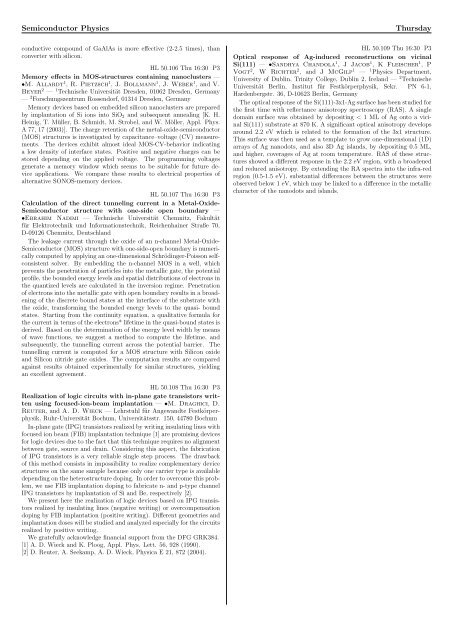
Memory effects in MOS-structures containing nanoclusters —<br />
•M. Allardt 1 , R. Pietzsch 1 , J. Bollmann 1 , J. Weber 1 , and V.<br />
Beyer 2 — 1 Technische Universität Dresden, 01062 Dresden, Germany<br />
— 2 Forschungszentrum Rossendorf, 01314 Dresden, Germany<br />
Memory devices based on embedded silicon nanoclusters are prepared<br />
by implantation of Si ions into SiO2 and subsequent annealing [K. H.<br />
Heinig, T. Müller, B. Schmidt, M. Strobel, and W. Möller, Appl. Phys.<br />
A 77, 17 (2003)]. The charge retention of the metal-oxide-semiconductor<br />
(MOS) structures is investigated by capacitance–voltage (CV) measurements.<br />
The devices exhibit almost ideal MOS-CV-behavior indicating<br />
a low density of interface states. Positive and negative charges can be<br />
stored depending on the applied voltage. The programming voltages<br />
generate a memory window which seems to be suitable for future device<br />
applications. We compare these results to electrical properties of<br />
alternative SONOS-memory devices.<br />
<strong>HL</strong> <strong>50</strong>.107 Thu 16:30 P3<br />
Calculation of the direct tunneling current in a Metal-Oxide-<br />
Semiconductor structure with one-side open boundary —<br />
•Ebrahim Nadimi — Technische Universität Chemnitz, Fakultät<br />
für Elektrotechnik und Informationstechnik, Reichenhainer Straße 70,<br />
D-09126 Chemnitz, Deutschland<br />
The leakage current through the oxide of an n-channel Metal-Oxide-<br />
Semiconductor (MOS) structure with one-side-open boundary is numerically<br />
computed by applying an one-dimensional Schrödinger-Poisson selfconsistent<br />
solver. By embedding the n-channel MOS in a well, which<br />
prevents the penetration of particles into the metallic gate, the potential<br />
profile, the bounded energy levels and spatial distributions of electrons in<br />
the quantized levels are calculated in the inversion regime. Penetration<br />
of electrons into the metallic gate with open boundary results in a broadening<br />
of the discrete bound states at the interface of the substrate with<br />
the oxide, transforming the bounded energy levels to the quasi- bound<br />
states. Starting from the continuity equation, a qualitative formula for<br />
the current in terms of the electrons* lifetime in the quasi-bound states is<br />
derived. Based on the determination of the energy level width by means<br />
of wave functions, we suggest a method to compute the lifetime, and<br />
subsequently, the tunnelling current across the potential barrier. The<br />
tunnelling current is computed for a MOS structure with Silicon oxide<br />
and Silicon nitride gate oxides. The computation results are compared<br />
against results obtained experimentally for similar structures, yielding<br />
an excellent agreement.<br />
<strong>HL</strong> <strong>50</strong>.108 Thu 16:30 P3<br />
Realization of logic circuits with in-plane gate transistors written<br />
using focused-ion-beam implantation — •M. Draghici, D.<br />
Reuter, and A. D. Wieck — Lehrstuhl für Angewandte Festkörperphysik,<br />
Ruhr-Universität Bochum, Universitätsstr. 1<strong>50</strong>, 44780 Bochum<br />
In-plane gate (IPG) transistors realized by writing insulating lines with<br />
focused ion beam (FIB) implantation technique [1] are promising devices<br />
for logic devices due to the fact that this technique requires no alignment<br />
between gate, source and drain. Considering this aspect, the fabrication<br />
of IPG transistors is a very reliable single step process. The drawback<br />
of this method consists in impossibility to realize complementary device<br />
structures on the same sample because only one carrier type is available<br />
depending on the heterostructure doping. In order to overcome this problem,<br />
we use FIB implantation doping to fabricate n- and p-type channel<br />
IPG transistors by implantation of Si and Be, respectively [2].<br />
We present here the realization of logic devices based on IPG transistors<br />
realized by insulating lines (negative writing) or overcompensation<br />
doping by FIB implantation (positive writing). Different geometries and<br />
implantation doses will be studied and analyzed especially for the circuits<br />
realized by positive writing.<br />
We gratefully acknowledge financial support from the DFG GRK384.<br />
[1] A. D. Wieck and K. Ploog, Appl. Phys. Lett. 56, 928 (1990).<br />
[2] D. Reuter, A. Seekamp, A. D. Wieck, Physica E 21, 872 (2004).<br />
<strong>HL</strong> <strong>50</strong>.109 Thu 16:30 P3<br />
Optical response of Ag-induced reconstructions on vicinal<br />
Si(111) — •Sandhya Chandola 1 , J Jacob 1 , K Fleischer 1 , P<br />
Vogt 2 , W Richter 2 , and J McGilp 1 — 1 Physics Department,<br />
University of Dublin, Trinity College, Dublin 2, Ireland — 2 Technische<br />
Universität Berlin, Institut für Festkörperphysik, Sekr. PN 6-1,<br />
Hardenbergstr. 36, D-10623 Berlin, Germany<br />
The optical response of the Si(111)-3x1-Ag surface has been studied for<br />
the first time with reflectance anisotropy spectroscopy (RAS). A single<br />
domain surface was obtained by depositing < 1 ML of Ag onto a vicinal<br />
Si(111) substrate at 870 K. A significant optical anisotropy develops<br />
around 2.2 eV which is related to the formation of the 3x1 structure.<br />
This surface was then used as a template to grow one-dimensional (1D)<br />
arrays of Ag nanodots, and also 3D Ag islands, by depositing 0.5 ML,<br />
and higher, coverages of Ag at room temperature. RAS of these structures<br />
showed a different response in the 2.2 eV region, with a broadened<br />
and reduced anisotropy. By extending the RA spectra into the infra-red<br />
region (0.5-1.5 eV), substantial differences between the structures were<br />
observed below 1 eV, which may be linked to a difference in the metallic<br />
character of the nanodots and islands.


