VIII.2. A Semiconductor Device Primer
VIII.2. A Semiconductor Device Primer
VIII.2. A Semiconductor Device Primer

Create successful ePaper yourself
Turn your PDF publications into a flip-book with our unique Google optimized e-Paper software.
<strong>VIII.2.</strong> A <strong>Semiconductor</strong> <strong>Device</strong> <strong>Primer</strong><br />
Bibliography:<br />
1. Grove, A.S., Physics and Technology of <strong>Semiconductor</strong><br />
<strong>Device</strong>s (John Wiley & Sons, New York, 1967)<br />
2. Sze, S.M., Physics of <strong>Semiconductor</strong> <strong>Device</strong>s (John Wiley &<br />
Sons, New York, 1981) TK 7871.85.S988, ISBN 0-471-05661-8<br />
3. Kittel, C., Introduction to Solid State Physics (John Wiley &<br />
Sons, New York, 1996) QC176.K5, ISBN 0-471-11181-3<br />
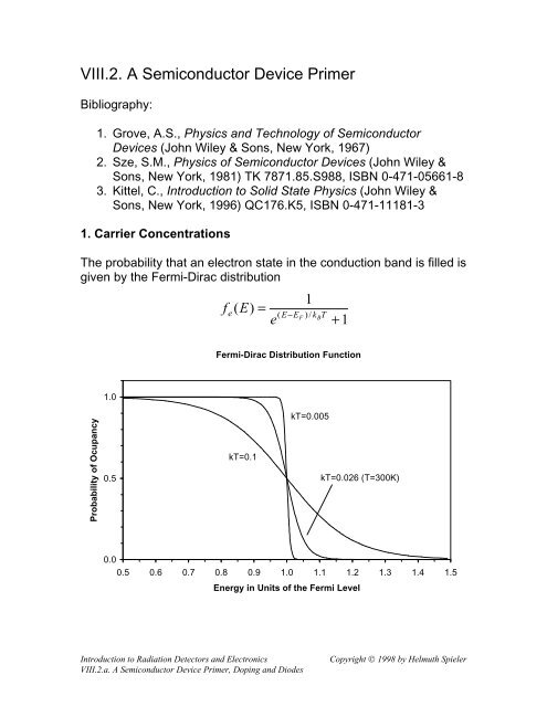
1. Carrier Concentrations<br />
The probability that an electron state in the conduction band is filled is<br />
given by the Fermi-Dirac distribution<br />
Probability of Ocupancy<br />
1.0<br />
0.5<br />
f<br />
e<br />
1<br />
( E)<br />
( E EF<br />
) /<br />
e<br />
= − k T<br />
+ 1<br />
Fermi-Dirac Distribution Function<br />
kT=0.1<br />
0.0<br />
0.5 0.6 0.7 0.8 0.9 1.0 1.1 1.2 1.3 1.4 1.5<br />
Energy in Units of the Fermi Level<br />
Introduction to Radiation Detectors and Electronics Copyright © 1998 by Helmuth Spieler<br />
<strong>VIII.2.</strong>a. A <strong>Semiconductor</strong> <strong>Device</strong> <strong>Primer</strong>, Doping and Diodes<br />
B<br />
kT=0.005<br />
kT=0.026 (T=300K)
The density of atoms in a Si or Ge crystal is about 4 . 10 22 atoms/cm 3 .<br />
Since the minimum carrier density of interest in practical devices is of<br />
order 10 10 to 10 11 cm -3 , very small ocupancy probabilities are quite<br />
important.<br />
Probability of Occupancy<br />
1.0E+00<br />
1.0E-02<br />
1.0E-04<br />
1.0E-06<br />
1.0E-08<br />
1.0E-10<br />
1.0E-12<br />
1.0E-14<br />
1.0E-16<br />
Fermi-Dirac Distribution Function<br />
kT=0.026 eV (T=300K)<br />
1.0E-18<br />
0.8 0.9 1 1.1 1.2 1.3 1.4 1.5 1.6 1.7 1.8 1.9 2<br />
Energy in Units of Fermi Level<br />
kT=0.035 eV (T=400K)<br />
In silicon the band gap is 1.12 eV. If the Fermi level is at midgap, the<br />
band-edges will be 0.56 eV above and below EF.<br />
As is apparent from the plot, relatively large deviations from the Fermi<br />
level, i.e. extremely small occupancies, will still yield significant carrier<br />
densities<br />
Introduction to Radiation Detectors and Electronics Copyright © 1998 by Helmuth Spieler<br />
<strong>VIII.2.</strong>a. A <strong>Semiconductor</strong> <strong>Device</strong> <strong>Primer</strong>, Doping and Diodes
The number of occupied electron states Ne is determined by<br />
summing over all available states multiplied by the occupation<br />
probability for each individual state<br />
∑<br />
N = m f ( E )<br />
Since the density of states near the band edge tends to be quite high,<br />
this can be written as an integral<br />
where g(E) is the density of states.<br />
e<br />
∞<br />
∫<br />
E<br />
i<br />
N = f ( E)<br />
g(<br />
E)<br />
dE<br />
e<br />
c<br />
Solution of this integral requires knowledge of the density of states.<br />
Fortuitously, to a good approximation the density of states near the<br />
band edge has a parabolic distribution<br />
( ) ( c ) E E dE E g − ∝<br />
As the energy increases beyond the band edge, the distribution will<br />
deviate from the simple parabolic form, but since the probability<br />
function decreases very rapidly, the integral will hardly be affected.<br />
The second obstacle to a simple analytical solution of the integral is<br />
the intractability of integrating over the Fermi distribution.<br />
i<br />
Introduction to Radiation Detectors and Electronics Copyright © 1998 by Helmuth Spieler<br />
<strong>VIII.2.</strong>a. A <strong>Semiconductor</strong> <strong>Device</strong> <strong>Primer</strong>, Doping and Diodes<br />
i<br />
1/<br />
2
Fortunately, if E-EF is at least several times kBT, the Fermi<br />
distribution can be approximated by a Boltzmann distribution<br />
Probability of Occupancy<br />
1<br />
0.1<br />
1+<br />
e<br />
( E−E ) / kBT<br />
( E−E<br />
F ) / kBT<br />
−(<br />
E−E<br />
F ) / kBT<br />
F ≈ e ⇒ f ( E)<br />
≈ e<br />
At energies beyond 2.3 kBT of the Fermi level the difference between<br />
the Boltzmann approximation and the Fermi Distribution is 4.5 kBT it is less than 1%.<br />
Applying the approximation to the occupancy of hole states, the<br />
probability of a hole state being occupied, i.e. a valence state being<br />
empty is<br />
f<br />
h<br />
( E)<br />
= 1−<br />
Fermi-Dirac Distribution vs. Boltzmann Approximation<br />
Fermi-Dirac Distribution<br />
f<br />
e<br />
( E)<br />
=<br />
Boltzmann Approximation<br />
0.01<br />
0.0 0.5 1.0 1.5 2.0 2.5 3.0 3.5 4.0 4.5<br />
Energy Spacing from Fermi Level in Units of kT<br />
e<br />
( E<br />
F<br />
−E<br />
) / k<br />
−E<br />
) / k<br />
Since the band gap is of order 1 eV and kBT at room temperature is<br />
0.026 eV, the conditions for the Boltzmann approximation are fulfilled<br />
for excitation across the band gap.<br />
Introduction to Radiation Detectors and Electronics Copyright © 1998 by Helmuth Spieler<br />
<strong>VIII.2.</strong>a. A <strong>Semiconductor</strong> <strong>Device</strong> <strong>Primer</strong>, Doping and Diodes<br />
1<br />
B<br />
T<br />
≈ e<br />
+ 1<br />
−(<br />
E<br />
F<br />
B<br />
T
With these simplifications the number of electrons in the conduction<br />
band in thermal equilibrium is<br />
or<br />
where Nc is the effective density of states at the band edge.<br />
Correspondingly, the hole concentration<br />
In a pure semiconductor<br />
where ni is the number of electrons or holes intrinsic to a pure<br />
semiconductor, i.e. where only source of mobile carriers is thermal<br />
excitation across the band gap without any additional impurity atoms<br />
or crystal imperfections that would allow other excitation<br />
mechanisms.<br />
Silicon (Eg = 1.12 eV): ni= 1.45 . 10 10 cm -3 at 300K<br />
Germanium (Eg = 0.66 eV): ni= 2.4 . 10 13 cm -3 at 300K<br />
For comparison:<br />
n<br />
n<br />
e<br />
e<br />
∝ ( k<br />
=<br />
p =<br />
N<br />
N<br />
c<br />
B<br />
v<br />
T )<br />
e<br />
3/<br />
2<br />
e<br />
−(<br />
E −E<br />
) / k T<br />
e<br />
c<br />
−(<br />
E<br />
n =<br />
p =<br />
F<br />
ni<br />
−(<br />
E −E<br />
) / k T<br />
The purest semiconductor material that has been fabricated<br />
is Ge with active impurity levels of about 3 . 10 10 cm -3 .<br />
F<br />
Introduction to Radiation Detectors and Electronics Copyright © 1998 by Helmuth Spieler<br />
<strong>VIII.2.</strong>a. A <strong>Semiconductor</strong> <strong>Device</strong> <strong>Primer</strong>, Doping and Diodes<br />
c<br />
B<br />
−E<br />
) / k T<br />
v<br />
B<br />
F<br />
B
Using the above results<br />
n<br />
i<br />
=<br />
N<br />
−(<br />
E −E<br />
) / k T<br />
which one can solve to obtain EF<br />
c<br />
e<br />
E<br />
c F B = N e<br />
+ E<br />
2<br />
k T<br />
2<br />
−E<br />
) / k T<br />
If the band structure is symmetrical (Nc=Nv), the intrinsic Fermi level<br />
lies in the middle of the band gap.<br />
Even rather substantial deviations from a symmetrical band structure<br />
will not affect this result significantly, as Nc /Nv enters logarithmically<br />
and kBT is much smaller than the band gap.<br />
A remarkable result is that the product of the electron and hole<br />
concentrations<br />
np =<br />
n<br />
depends only on the band gap Eg and not on the Fermi level.<br />
This result, the law of mass action, is very useful in semiconductor<br />
device analysis. It requires only that the Boltzmann approximation<br />
holds.<br />
Qualitatively, it says that if one carrier type exceeds this equilibrium<br />
concentration, recombination will decrease the concentrations of both<br />
electrons and holes to maintain np= ni 2 .<br />
Introduction to Radiation Detectors and Electronics Copyright © 1998 by Helmuth Spieler<br />
<strong>VIII.2.</strong>a. A <strong>Semiconductor</strong> <strong>Device</strong> <strong>Primer</strong>, Doping and Diodes<br />
v<br />
−(<br />
E<br />
F<br />
v<br />
B<br />
( N N )<br />
c v B<br />
E F = − log c /<br />
2<br />
i<br />
=<br />
N<br />
c<br />
N<br />
v<br />
e<br />
−(<br />
E −E<br />
) / k T<br />
c v B = N N e<br />
c<br />
v<br />
v<br />
−E<br />
/ k T<br />
g<br />
B
2. Carrier Concentrations in Doped Crystals<br />
The equality<br />
ne = nh<br />
only holds for pure crystals, where all of the electrons in the<br />
conduction band have been thermally excited from the valence band.<br />
In practical semiconductors the presence of impurities tips the<br />
balance towards either the electrons or holes.<br />
Impurities are an unavoidable byproduct of the crystal growth<br />
process, although special techniques can achieve astounding results.<br />
For example, in the purest semiconductor crystals – “ultrapure” Ge –<br />
the net impurity concentration is about 3 . 10 10 cm -3 .<br />
In semiconductor device technology impurities are introduced<br />
intentionally to control the conductivity of the semiconductor.<br />
Let Nd + be the concentration of ionized donors and Na - the<br />
concentration of ionized acceptors.<br />
Overall charge neutrality is preserved, as each ionized dopant<br />
introduces a charged carrier and an oppositely charged atom, but the<br />
net carrier concentration is now<br />
or<br />
Assume that the activation energy of the donors and acceptors is<br />
sufficiently small so that they are fully ionized<br />
Then<br />
+<br />
D<br />
+ −<br />
Δn = n − p = N d − Na<br />
p<br />
+<br />
−<br />
+ N D = n + N A<br />
D<br />
Introduction to Radiation Detectors and Electronics Copyright © 1998 by Helmuth Spieler<br />
<strong>VIII.2.</strong>a. A <strong>Semiconductor</strong> <strong>Device</strong> <strong>Primer</strong>, Doping and Diodes<br />
−<br />
A<br />
N ≈ N and N ≈<br />
p +<br />
N = n + N<br />
D<br />
A<br />
,<br />
N<br />
A
which, using np= ni 2 , becomes<br />
If the acceptor concentration NA >> ND and NA >> ni<br />
i.e. the conductivity is dominated by holes.<br />
Conversely, if the donor concentration ND >> NA and ND >> ni the<br />
conductivity is dominated by electrons.<br />
If the conductivity is dominated by only one type of carrier, the Fermi<br />
level is easy to determine. If, for example, n >> p<br />
can be written<br />
yielding<br />
p<br />
N<br />
A<br />
N<br />
+<br />
N<br />
D<br />
A<br />
2<br />
ni<br />
p + N D = +<br />
ni<br />
ni<br />
=<br />
p N<br />
N<br />
c<br />
e<br />
Ec<br />
− E<br />
k T<br />
B<br />
A<br />
+ 1<br />
D<br />
− ( E −E<br />
) / k<br />
p<br />
T<br />
⇒<br />
If ND >> NA , then Ec-EF must be small, i.e. the Fermi level lies close<br />
to the conduction band edge.<br />
In reality the impurity levels of common dopants are not close enough<br />
to the band edge for the Boltzmann approximation to hold, so the<br />
calculation must use the Fermi distribution and solve numerically for<br />
EF. Nevertheless, the qualitative conclusions derived here still apply.<br />
Introduction to Radiation Detectors and Electronics Copyright © 1998 by Helmuth Spieler<br />
<strong>VIII.2.</strong>a. A <strong>Semiconductor</strong> <strong>Device</strong> <strong>Primer</strong>, Doping and Diodes<br />
N<br />
p + N = n + N<br />
N N n − =<br />
F<br />
D<br />
A<br />
A<br />
A<br />
D<br />
p ≈<br />
c F B = N − N<br />
⎛<br />
= log<br />
⎜<br />
⎝ N<br />
D<br />
N c<br />
− N<br />
A<br />
N<br />
A<br />
⎞<br />
⎟<br />
⎠<br />
A<br />
,<br />
2<br />
i<br />
n<br />
n ≈<br />
N<br />
A<br />
It is often convenient to refer all of these quantities to the intrinsic<br />
level Ei , as it accounts for both Ec and Ev. Then<br />
n =<br />
p =<br />
N<br />
N<br />
and the Fermi level<br />
E<br />
F<br />
c<br />
v<br />
e<br />
e<br />
−(<br />
Ec−<br />
EF<br />
) / kBT<br />
−(<br />
EF<br />
−Ei<br />
) / k<br />
= nie<br />
−(<br />
EF<br />
−Ev<br />
) / kBT<br />
−(<br />
Ei<br />
−E<br />
= nie<br />
N<br />
− E = −k<br />
T log<br />
i<br />
B<br />
Variation of Fermi level with doping and temperature, including<br />
narrowing of the band gap with temperature:<br />
(from Sze)<br />
Introduction to Radiation Detectors and Electronics Copyright © 1998 by Helmuth Spieler<br />
<strong>VIII.2.</strong>a. A <strong>Semiconductor</strong> <strong>Device</strong> <strong>Primer</strong>, Doping and Diodes<br />
A<br />
i<br />
F<br />
− N<br />
n<br />
B<br />
) / k<br />
D<br />
B<br />
T<br />
T
3. p-n Junctions<br />
A p-n junction is formed at the interface of a p- and an n-type region.<br />
(from Kittel)<br />
Since the electron concentration in the n-region is greater than in the<br />
p-region, electrons will diffuse into the p-region.<br />
Correspondingly, holes will diffuse into the n-region.<br />
As electrons and holes diffuse across the junction, a space charge<br />
due to the ionized donor and acceptor atoms builds up. The field due<br />
to this space charge is directed to impede the flow of electrons and<br />
holes.<br />
The situation is dynamic:<br />
The concentration gradient causes a continuous diffusion current<br />
to flow.<br />
The field due to the space charge drives a drift current in the<br />
opposite direction.<br />
Introduction to Radiation Detectors and Electronics Copyright © 1998 by Helmuth Spieler<br />
<strong>VIII.2.</strong>a. A <strong>Semiconductor</strong> <strong>Device</strong> <strong>Primer</strong>, Doping and Diodes
Equilibrium is attained when the two currents are equal, i.e. the sum<br />
of the diffusion and drift currents is zero.<br />
The net hole current density is<br />
where Dp is the diffusion constant for holes and Ep is the electric field<br />
in the p-region.<br />
To solve this equation we make use of the following relationships:<br />
The hole concentration is<br />
so its derivative<br />
dp<br />
J p = −qeD<br />
p + qe<br />
pμ<br />
dx<br />
p = n e<br />
dx<br />
=<br />
i<br />
( E −E<br />
) / k T<br />
i<br />
dp F<br />
F<br />
p ⎛ dEi<br />
⎜<br />
kT ⎝ dx<br />
Since the force on a charge qe due to an electric field E is equal to<br />
the negative gradient of the potential energy,<br />
dEc<br />
qeE<br />
=<br />
−<br />
dx<br />
As only the gradient is of interest and Ec , Ev and Ei differ only by a<br />
constant offset, any of these three measures can be used. We’ll use<br />
the intrinsic Fermi level Ei since it applies throughout the sample.<br />
The remaining ingredient is the Einstein relationship, which relates<br />
the mobility to the diffusion constant<br />
μ p =<br />
Introduction to Radiation Detectors and Electronics Copyright © 1998 by Helmuth Spieler<br />
<strong>VIII.2.</strong>a. A <strong>Semiconductor</strong> <strong>Device</strong> <strong>Primer</strong>, Doping and Diodes<br />
B<br />
,<br />
dE<br />
−<br />
dx<br />
dE<br />
= −<br />
dx<br />
q<br />
e<br />
k<br />
D<br />
B<br />
v<br />
T<br />
p<br />
⎞<br />
⎟<br />
⎠<br />
p<br />
E<br />
p<br />
dEi<br />
= −<br />
dx
Using these relationships the net hole current becomes<br />
= q<br />
Dp<br />
dEF<br />
p<br />
k T dx<br />
Accordingly, the net electron current<br />
J<br />
J<br />
Since, individually, the net hole and electron currents in equilibrium<br />
must be zero, the derivative of the Fermi level<br />
⇒ in thermal equilibrium the Fermi level must be constant<br />
throughout the junction region.<br />
For the Fermi level to be flat, the band structure must adapt, since on<br />
the p-side the Fermi level is near the valence band, whereas on the<br />
n-side it is near the conduction band.<br />
If we assume that the dopants are exclusively donors on the n-side<br />
and acceptors on the p-side, the difference in the respective Fermi<br />
levels is<br />
This corresponds to an electric potential<br />
p<br />
n<br />
e<br />
dE<br />
p<br />
dx<br />
often referred to as the “built-in” voltage of the junction.<br />
B<br />
Dn<br />
dEF<br />
= −qen<br />
k T dx<br />
ΔE<br />
= −k<br />
F<br />
B<br />
B<br />
dEF dx<br />
= μ<br />
= 0<br />
N<br />
T log<br />
1<br />
ΔVF<br />
= ΔEF<br />
≡ V<br />
q<br />
Introduction to Radiation Detectors and Electronics Copyright © 1998 by Helmuth Spieler<br />
<strong>VIII.2.</strong>a. A <strong>Semiconductor</strong> <strong>Device</strong> <strong>Primer</strong>, Doping and Diodes<br />
p<br />
= −μ<br />
N<br />
A D<br />
2<br />
ni<br />
bi<br />
n<br />
F<br />
dE<br />
n<br />
dx<br />
F
As either NA or ND increases relative to ni, the respective Fermi level<br />
moves closer to the band edge, increasing the built-in voltage.<br />
With increasing doping levels the built-in voltage approaches the<br />
equivalent potential of the band-gap Eg /qe.<br />
(from Sze)<br />
Introduction to Radiation Detectors and Electronics Copyright © 1998 by Helmuth Spieler<br />
<strong>VIII.2.</strong>a. A <strong>Semiconductor</strong> <strong>Device</strong> <strong>Primer</strong>, Doping and Diodes
The inherent potential distribution in the junction leads to a depletion<br />
region, whose width can be increased by application of an external<br />
potential, i.e. reverse biasing the junction.<br />
This was discussed in a previous lecture.<br />
Now the forward bias mode will be treated in more detail.<br />
Complication:<br />
(from Kittel)<br />
Applying an external bias leads to a condition that deviates from<br />
thermal equilibrium, i.e. the Fermi level is no longer constant<br />
throughout the junction.<br />
Introduction to Radiation Detectors and Electronics Copyright © 1998 by Helmuth Spieler<br />
<strong>VIII.2.</strong>a. A <strong>Semiconductor</strong> <strong>Device</strong> <strong>Primer</strong>, Doping and Diodes
4. The Forward-Biased p-n Junction<br />
If a positive voltage is applied to the p-electrode relative to the<br />
n-electrode, the total variation of the electric potential across the<br />
junction will decrease.<br />
(from Kittel)<br />
Since this reduces the electric field across the junction, the drift<br />
component of the junction current will decrease. Since the<br />
concentration gradient is unchanged, the diffusion current will exceed<br />
the drift current and a net current will flow.<br />
This net current leads to an excess of electrons in the p-region and<br />
an excess of holes in the n-region. This “injection” condition lead to<br />
a local deviation from equilibrium, i.e. pn>ni 2 . Equilibrium will be<br />
restored by recombination.<br />
Note that a depletion region exists even under forward bias,<br />
although its width is decreased. The electric field due to the space<br />
charge opposes the flow of charge, but the large concentration<br />
gradient overrides the field.<br />
Introduction to Radiation Detectors and Electronics Copyright © 1998 by Helmuth Spieler<br />
<strong>VIII.2.</strong>a. A <strong>Semiconductor</strong> <strong>Device</strong> <strong>Primer</strong>, Doping and Diodes
Consider holes flowing into the n-region. They will flow through the<br />
depletion region with small losses due to recombination, as the<br />
electron concentration is small compared with the bulk.<br />
When holes reach the n-side boundary of the depletion region the<br />
concentration of electrons available for recombination increases and<br />
the concentration of holes will decrease with distance, depending on<br />
the cross-section for recombination, expressed as a diffusion length.<br />
Ultimately, all holes will have recombined with electrons. The required<br />
electrons are furnished through the external contact from the power<br />
supply.<br />
On the p-side, electrons undergo a similar process. The holes<br />
required to sustain recombination are formed at the external contact<br />
to the p-region by electron flow toward the power supply, equal to the<br />
electron flow toward the n-contact.<br />
The steady-state distribution of charge is determined by solving the<br />
diffusion equation.<br />
D<br />
n<br />
d<br />
2<br />
n p<br />
2<br />
dx<br />
n<br />
−<br />
p<br />
− n<br />
τ<br />
= 0<br />
Electrons flowing into the p region give rise to a local concentration np<br />
in excess of the equilibrium concentration np0. This excess will decay<br />
with a recombination time τn, corresponding to a diffusion length Ln.<br />
The first boundary condition required for the solution of the diffusion<br />
equation is that the excess concentration of electrons vanish at large<br />
distances x,<br />
n =<br />
The second boundary condition is that the carriers are injected at the<br />
origin of the space charge region x= 0 with a concentration np(0).<br />
Introduction to Radiation Detectors and Electronics Copyright © 1998 by Helmuth Spieler<br />
<strong>VIII.2.</strong>a. A <strong>Semiconductor</strong> <strong>Device</strong> <strong>Primer</strong>, Doping and Diodes<br />
n<br />
p ( ∞)<br />
n p0<br />
p0
This yields the solution<br />
n<br />
p<br />
( x)<br />
= n<br />
p0<br />
n<br />
( ) L x − /<br />
n ( 0)<br />
− n e<br />
From this we obtain the electron current entering the p-region<br />
J<br />
np<br />
= −q<br />
e<br />
D<br />
This says that the electron current is limited by the concentration<br />
gradient determined by the carrier density at the depletion edge np(0)<br />
and the equilibrium minority carrier density np0 .<br />
Determining the equilibrium minority np0 is easy<br />
n<br />
dn<br />
dx<br />
+<br />
p<br />
x=<br />
0<br />
The problem is that np(0) is established in a non-equilibrium state,<br />
where the previously employed results do not apply.<br />
p<br />
= q<br />
To analyze the regions with non-equilibrium carrier concentrations<br />
a simplifying assumption is made by postulating that the product<br />
pn is constant. In this specific quasi-equilibrium state this constant<br />
will be larger than ni 2 , the pn-product in thermal equilibrium.<br />
In analogy to thermal equilibrium, this quasi-equilibrium state is<br />
expressed in terms of a “quasi-Fermi level”, which is the quantity<br />
used in place of EF that gives the carrier concentration under nonequilibrium<br />
conditions.<br />
2<br />
i<br />
Introduction to Radiation Detectors and Electronics Copyright © 1998 by Helmuth Spieler<br />
<strong>VIII.2.</strong>a. A <strong>Semiconductor</strong> <strong>Device</strong> <strong>Primer</strong>, Doping and Diodes<br />
e<br />
n n / N<br />
p0<br />
=<br />
D<br />
A<br />
n<br />
p0<br />
n<br />
p<br />
( 0)<br />
− n<br />
L<br />
n<br />
p0
The postulate pn= const. is equivalent to stating that the nonequilibrium<br />
carrier concentrations are given by a Boltzmann<br />
distribution, so the concentration of electrons is<br />
n = n e<br />
( E −E<br />
) / k<br />
where EFn is the quasi-Fermi level for electrons, and<br />
where EFp is the quasi-Fermi level for holes.<br />
i<br />
p = n e<br />
i<br />
Fn<br />
( E −E<br />
The product of the two carrier concentration in non-equilibrium is<br />
2<br />
i<br />
pn = n<br />
e<br />
( E<br />
Fn<br />
i<br />
−E<br />
Fp<br />
If pn is constant throughout the space-charge region, then EFn-EFp<br />
must also remain constant.<br />
Using the quasi-Fermi level and the Einstein relationship, the electron<br />
current entering the p-region becomes<br />
J<br />
np<br />
= −q<br />
e<br />
D<br />
n<br />
dn<br />
dx<br />
p<br />
x=<br />
0<br />
= − − q<br />
e<br />
D<br />
n<br />
These relationships describe the behavior of the quasi-Fermi level in<br />
the depletion region. How does this connect to the neutral region?<br />
In the neutral regions the majority carrier motion is dominated by drift<br />
(in contrast to the injected minority carrier current that is determined<br />
by difusion). Consider the n-type region. Here the bulk electron<br />
current that provides the junction current<br />
J<br />
nn<br />
=<br />
−μ<br />
n<br />
Introduction to Radiation Detectors and Electronics Copyright © 1998 by Helmuth Spieler<br />
<strong>VIII.2.</strong>a. A <strong>Semiconductor</strong> <strong>Device</strong> <strong>Primer</strong>, Doping and Diodes<br />
i<br />
Fp<br />
) / k<br />
d<br />
dx<br />
B<br />
) / k<br />
B<br />
T<br />
dEi<br />
n<br />
dx<br />
B<br />
T<br />
T<br />
( n e<br />
i<br />
( E<br />
−E<br />
) / k<br />
T<br />
Fn i B ) = −μ<br />
n<br />
dE<br />
n<br />
dx<br />
Fn
Since the two electron currents must be equal<br />
it follows that<br />
i.e. the quasi-Fermi level follows the energy band variation.<br />
⇒ in a neutral region, the quasi-Fermi level for the majority<br />
carriers is the same as the Fermi level in equilibrium.<br />
At current densities small enough not to cause significant voltage<br />
drops in the neutral regions, the band diagram is flat, and hence the<br />
quasi-Fermi level is flat.<br />
In the space charge region, pn is constant, so the quasi-Fermi levels<br />
for holes and electrons must be parallel, i.e. both will remain constant<br />
at their respective majority carrier equilibrium levels in the neutral<br />
regions.<br />
If an external bias V is applied, the equilibrium Fermi levels are offset<br />
by V, so it follows that the quasi-Fermi levels are also offset by V.<br />
EFn − EFp<br />
= qeV<br />
Consequently, the pn-product in non-equilibrium<br />
pn = n<br />
2<br />
i<br />
J =<br />
e<br />
nn<br />
( E<br />
Fn<br />
−E<br />
J<br />
Fp<br />
np<br />
dEFn i =<br />
dx<br />
dE<br />
dx<br />
) / k<br />
q V / k<br />
Introduction to Radiation Detectors and Electronics Copyright © 1998 by Helmuth Spieler<br />
<strong>VIII.2.</strong>a. A <strong>Semiconductor</strong> <strong>Device</strong> <strong>Primer</strong>, Doping and Diodes<br />
B<br />
T<br />
= n<br />
2<br />
i<br />
e<br />
e<br />
B<br />
T
If the majority carrier concentration is much greater than the<br />
concentration due to minority injection (“low-level injection”), the hole<br />
concentration at the edge of the p-region remains essentially at the<br />
equilibrium value. Consequently, the enhanced pn-product increases<br />
the electron concentration.<br />
n<br />
p<br />
( 0)<br />
= n<br />
p0<br />
q V / k<br />
Correspondingly, the hole concentration in the n-region at the edge of<br />
the depletion zone becomes<br />
p ( 0)<br />
=<br />
p<br />
n<br />
n0<br />
Introduction to Radiation Detectors and Electronics Copyright © 1998 by Helmuth Spieler<br />
<strong>VIII.2.</strong>a. A <strong>Semiconductor</strong> <strong>Device</strong> <strong>Primer</strong>, Doping and Diodes<br />
e<br />
e<br />
e<br />
B<br />
q V / k<br />
e<br />
B<br />
T<br />
T
Energy band diagrams showing the intrinsic Fermi level Ψ,<br />
the quasi-Fermi levels for electrons Φn and holes Φp , and the<br />
carrier distributions for forward (a) and reverse bias conditions (b).<br />
p n p n<br />
forward bias reverse bias<br />
(from Sze)<br />
Introduction to Radiation Detectors and Electronics Copyright © 1998 by Helmuth Spieler<br />
<strong>VIII.2.</strong>a. A <strong>Semiconductor</strong> <strong>Device</strong> <strong>Primer</strong>, Doping and Diodes
Carrier distributions and current densities for forward (a) and<br />
reverse bias conditions (b)<br />
p n p n<br />
forward bias reverse bias<br />
(from Sze)<br />
Introduction to Radiation Detectors and Electronics Copyright © 1998 by Helmuth Spieler<br />
<strong>VIII.2.</strong>a. A <strong>Semiconductor</strong> <strong>Device</strong> <strong>Primer</strong>, Doping and Diodes
Since the equilibrium concentrations<br />
the components of the diffusion current due to holes and electrons<br />
are<br />
The total current is the sum of the electron and hole components<br />
where<br />
J<br />
J<br />
n<br />
p<br />
J<br />
n<br />
p0<br />
e<br />
e<br />
2<br />
i<br />
n<br />
=<br />
N<br />
= q D<br />
n<br />
= q D<br />
J<br />
=<br />
0<br />
J<br />
n<br />
p<br />
+ J<br />
= q n<br />
e<br />
A<br />
2<br />
i<br />
n<br />
N L<br />
A<br />
D<br />
2<br />
i<br />
n<br />
n<br />
N L<br />
2<br />
i<br />
p<br />
=<br />
and<br />
p<br />
J<br />
Introduction to Radiation Detectors and Electronics Copyright © 1998 by Helmuth Spieler<br />
<strong>VIII.2.</strong>a. A <strong>Semiconductor</strong> <strong>Device</strong> <strong>Primer</strong>, Doping and Diodes<br />
p<br />
n0<br />
2<br />
i<br />
n<br />
=<br />
N<br />
qeV<br />
/ kBT<br />
( e −1)<br />
qeV<br />
/ kBT<br />
( e −1)<br />
0<br />
⎛<br />
⎜<br />
Dn<br />
⎜<br />
⎝ N AL<br />
( e<br />
n<br />
q V / k T<br />
+<br />
e<br />
N<br />
B<br />
D<br />
D<br />
p<br />
L<br />
−1)<br />
p<br />
⎞<br />
⎟<br />
⎠<br />
D
Forward and reverse characteristics of a pn-junction diode<br />
(from Sze)<br />
Introduction to Radiation Detectors and Electronics Copyright © 1998 by Helmuth Spieler<br />
<strong>VIII.2.</strong>a. A <strong>Semiconductor</strong> <strong>Device</strong> <strong>Primer</strong>, Doping and Diodes
Note that in the diode equation<br />
a) The band gap does not appear explicitly<br />
(only implicitly via ni )<br />
b) The total current has two distinct components, due to electrons<br />
and holes.<br />
c) The electron and hole currents are not necessarily equal<br />
I<br />
I<br />
n<br />
p<br />
N<br />
=<br />
N<br />
D<br />
A<br />
if<br />
d) Current flows for all values of V. However, when plotted on a<br />
linear scale, the exponential appears to have a knee, often<br />
referred to as the “turn-on” voltage<br />
e) The magnitude of the turn-on voltage is determined by I0.<br />
Diodes with different band-gaps will show the same behavior if<br />
I0 is the same.<br />
Introduction to Radiation Detectors and Electronics Copyright © 1998 by Helmuth Spieler<br />
<strong>VIII.2.</strong>a. A <strong>Semiconductor</strong> <strong>Device</strong> <strong>Primer</strong>, Doping and Diodes<br />
D<br />
L<br />
n<br />
n<br />
=<br />
D<br />
L<br />
p<br />
p
Comparision between commercial Si and Ge junction diodes<br />
(1N4148 and 1N34A)<br />
Forward Current [A]<br />
1.4E-02<br />
1.2E-02<br />
1.0E-02<br />
8.0E-03<br />
6.0E-03<br />
4.0E-03<br />
2.0E-03<br />
0.0E+00<br />
Si and Ge Diodes - Forward Bias<br />
0 200 400 600 800 1000<br />
Forward Voltage [mV]<br />
On a linear scale the Ge diode “turns on” at 200 – 300 mV, whereas<br />
the Si diode has a threshold of 500 – 600 mV<br />
Introduction to Radiation Detectors and Electronics Copyright © 1998 by Helmuth Spieler<br />
<strong>VIII.2.</strong>a. A <strong>Semiconductor</strong> <strong>Device</strong> <strong>Primer</strong>, Doping and Diodes<br />
Ge<br />
Si
However, on a logarithmic scale it becomes apparent that both<br />
diodes pass current at all voltages >0.<br />
Forward Current [A]<br />
1.0E-01<br />
1.0E-02<br />
1.0E-03<br />
1.0E-04<br />
1.0E-05<br />
1.0E-06<br />
1.0E-07<br />
1.0E-08<br />
1.0E-09<br />
1.0E-10<br />
1.0E-11<br />
Si vs. Ge Diode - Forward Bias<br />
0 200 400 600 800 1000<br />
Forward Voltage [mV]<br />
The reverse current shows why the Ge diode shows greater<br />
sensitivity at low voltages (smaller band-gap ⇒ increased ni).<br />
Reverse Current [A]<br />
1.0E-05<br />
1.0E-06<br />
1.0E-07<br />
1.0E-08<br />
1.0E-09<br />
Ge<br />
Si<br />
Si vs. Ge Diodes - Reverse Bias<br />
Si<br />
0 2 4 6 8 10<br />
Reverse Voltage [V]<br />
Introduction to Radiation Detectors and Electronics Copyright © 1998 by Helmuth Spieler<br />
<strong>VIII.2.</strong>a. A <strong>Semiconductor</strong> <strong>Device</strong> <strong>Primer</strong>, Doping and Diodes<br />
Ge
The Si diode shows a “textbook” exponential forward characteristic at<br />
currents >10 nA, whereas the Ge diode exhibits a more complex<br />
structure.<br />
A “state-of-the-art” reverse diode characteristic (Steve Holland)<br />
Reverse Bias Current [pA]<br />
50<br />
40<br />
30<br />
20<br />
10<br />
0<br />
0 10 20 30 40 50 60 70 80 90 100<br />
Reverse Bias Voltage [V]<br />
The depletion width is 300 μm, attained at about 20 V.<br />
The area of the diode is 9 mm 2 , so the reverse leakage current of<br />
40 pA corresponds to 450 pA/cm 2 , which is about 10x the theoretical<br />
value.<br />
Introduction to Radiation Detectors and Electronics Copyright © 1998 by Helmuth Spieler<br />
<strong>VIII.2.</strong>a. A <strong>Semiconductor</strong> <strong>Device</strong> <strong>Primer</strong>, Doping and Diodes
The discrepancies between the measured results and the simple<br />
theory require the analysis of additional processes in the depletion<br />
zone.<br />
One can recognize four regions in the forward current:<br />
a) generation- recombination in the depletion region<br />
b) diffusion current (as just calculated for the ideal diode)<br />
c) high-injection region where the injected carrier concentration<br />
affects the potentials in the neutral regions.<br />
d) voltage drop due to bulk series resistance<br />
The reverse current is increased due to generation currents in the<br />
depletion zone.<br />
Introduction to Radiation Detectors and Electronics Copyright © 1998 by Helmuth Spieler<br />
<strong>VIII.2.</strong>a. A <strong>Semiconductor</strong> <strong>Device</strong> <strong>Primer</strong>, Doping and Diodes