What Every Programmer Should Know About Memory
What Every Programmer Should Know About Memory
What Every Programmer Should Know About Memory

You also want an ePaper? Increase the reach of your titles
YUMPU automatically turns print PDFs into web optimized ePapers that Google loves.
than the CPU core to one or two orders of magnitude<br />
slower.<br />
2.2 DRAM Access Technical Details<br />
In the section introducing DRAM we saw that DRAM<br />
chips multiplex the addresses in order to save resources<br />
int the form of address pins. We also saw that accessing<br />
DRAM cells takes time since the capacitors in those<br />
cells do not discharge instantaneously to produce a stable<br />
signal; we also saw that DRAM cells must be refreshed.<br />
Now it is time to put this all together and see how all<br />
these factors determine how the DRAM access has to<br />
happen.<br />
We will concentrate on current technology; we will not<br />
discuss asynchronous DRAM and its variants as they are<br />
simply not relevant anymore. Readers interested in this<br />
topic are referred to [3] and [19]. We will also not talk<br />
about Rambus DRAM (RDRAM) even though the technology<br />
is not obsolete. It is just not widely used for system<br />
memory. We will concentrate exclusively on Synchronous<br />
DRAM (SDRAM) and its successors Double<br />
Data Rate DRAM (DDR).<br />
Synchronous DRAM, as the name suggests, works relative<br />
to a time source. The memory controller provides<br />
a clock, the frequency of which determines the speed of<br />
the Front Side Bus (FSB) – the memory controller interface<br />
used by the DRAM chips. As of this writing,<br />
frequencies of 800MHz, 1,066MHz, or even 1,333MHz<br />
are available with higher frequencies (1,600MHz) being<br />
announced for the next generation. This does not mean<br />
the frequency used on the bus is actually this high. Instead,<br />
today’s buses are double- or quad-pumped, meaning<br />
that data is transported two or four times per cycle.<br />
Higher numbers sell so the manufacturers like to<br />
advertise a quad-pumped 200MHz bus as an “effective”<br />
800MHz bus.<br />
For SDRAM today each data transfer consists of 64 bits<br />
– 8 bytes. The transfer rate of the FSB is therefore 8<br />
bytes multiplied by the effective bus frequency (6.4GB/s<br />
for the quad-pumped 200MHz bus). That sounds a lot<br />
but it is the burst speed, the maximum speed which will<br />
never be surpassed. As we will see now the protocol for<br />
talking to the RAM modules has a lot of downtime when<br />
no data can be transmitted. It is exactly this downtime<br />
which we must understand and minimize to achieve the<br />
best performance.<br />
2.2.1 Read Access Protocol<br />
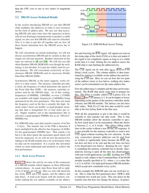
Figure 2.8 shows the activity on some of the connectors<br />
of a DRAM module which happens in three differently<br />
colored phases. As usual, time flows from left to right.<br />
A lot of details are left out. Here we only talk about the<br />
bus clock, RAS and CAS signals, and the address and<br />
data buses. A read cycle begins with the memory controller<br />
making the row address available on the address<br />
CLK<br />
RAS<br />
CAS<br />
Address<br />
DQ<br />
Row<br />
Addr<br />
t RCD<br />
Col<br />
Addr<br />
CL<br />
Data<br />
Out<br />
Data<br />
Out<br />
Data<br />
Figure 2.8: SDRAM Read Access Timing<br />
bus and lowering the RAS signal. All signals are read on<br />
the rising edge of the clock (CLK) so it does not matter if<br />
the signal is not completely square as long as it is stable<br />
at the time it is read. Setting the row address causes the<br />
RAM chip to start latching the addressed row.<br />
The CAS signal can be sent after t RCD (RAS-to-CAS<br />
Delay) clock cycles. The column address is then transmitted<br />
by making it available on the address bus and lowering<br />
the CAS line. Here we can see how the two parts<br />
of the address (more or less halves, nothing else makes<br />
sense) can be transmitted over the same address bus.<br />
Now the addressing is complete and the data can be transmitted.<br />
The RAM chip needs some time to prepare for<br />
this. The delay is usually called CAS Latency (CL). In<br />
Figure 2.8 the CAS latency is 2. It can be higher or lower,<br />
depending on the quality of the memory controller, motherboard,<br />
and DRAM module. The latency can also have<br />
half values. With CL=2.5 the first data would be available<br />
at the first falling flank in the blue area.<br />
With all this preparation to get to the data it would be<br />
wasteful to only transfer one data word. This is why<br />
DRAM modules allow the memory controller to specify<br />
how much data is to be transmitted. Often the choice<br />
is between 2, 4, or 8 words. This allows filling entire<br />
lines in the caches without a new RAS/CAS sequence. It<br />
is also possible for the memory controller to send a new<br />
CAS signal without resetting the row selection. In this<br />
way, consecutive memory addresses can be read from<br />
or written to significantly faster because the RAS signal<br />
does not have to be sent and the row does not have<br />
to be deactivated (see below). Keeping the row “open”<br />
is something the memory controller has to decide. Speculatively<br />
leaving it open all the time has disadvantages<br />
with real-world applications (see [3]). Sending new CAS<br />
signals is only subject to the Command Rate of the RAM<br />
module (usually specified as Tx, where x is a value like<br />
1 or 2; it will be 1 for high-performance DRAM modules<br />
which accept new commands every cycle).<br />
In this example the SDRAM spits out one word per cycle.<br />
This is what the first generation does. DDR is able<br />
to transmit two words per cycle. This cuts down on the<br />
transfer time but does not change the latency. In princi-<br />
8 Version 1.0 <strong>What</strong> <strong>Every</strong> <strong>Programmer</strong> <strong>Should</strong> <strong>Know</strong> <strong>About</strong> <strong>Memory</strong><br />
Out<br />
Data<br />
Out