

Next-Generation MMIC Design with Taiyo Yuden and UMS
Next-Generation MMIC Design with Taiyo Yuden and UMS
Next-Generation MMIC Design with Taiyo Yuden and UMS

You also want an ePaper? Increase the reach of your titles
YUMPU automatically turns print PDFs into web optimized ePapers that Google loves.
Page-14<br />
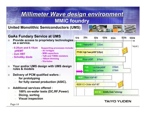
Millimeter Wave design environment<br />
<strong>MMIC</strong> foundry<br />
United Monolithic Semiconductors (<strong>UMS</strong>)<br />
GaAs Fundary Service at <strong>UMS</strong><br />
� Provide access to proprietary technologies<br />
as a service.<br />
- 0.25um <strong>and</strong> 0.15um<br />
pHEMT<br />
- 2um HBT<br />
- Schottky diode<br />
Supporting processes include:<br />
- Air bridges<br />
- MIM capacitors<br />
- TaN <strong>and</strong> TiWSi resistors<br />
- 100um thinning<br />
- Via-holes<br />
� Your <strong>and</strong>/or <strong>UMS</strong> design <strong>with</strong> <strong>UMS</strong> design<br />
rules & models<br />
� Delivery of PCM qualified wafers :<br />
– for prototyping<br />
– for fully owned production (ASIC).<br />
� Additional services offered :<br />
– 100% on-wafer tests (DC,RF,Power)<br />
– Dicing, sorting<br />
– Visual inspection


