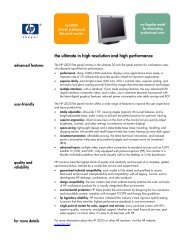
Understanding pixel defects in TFT-LCD flat panel monitors
Understanding pixel defects in TFT-LCD flat panel monitors
Understanding pixel defects in TFT-LCD flat panel monitors

Create successful ePaper yourself
Turn your PDF publications into a flip-book with our unique Google optimized e-Paper software.
<strong>Understand<strong>in</strong>g</strong> <strong>pixel</strong> <strong>defects</strong> <strong>in</strong> <strong>TFT</strong>-<strong>LCD</strong> <strong>flat</strong> <strong>panel</strong> <strong>monitors</strong><br />
Introduction......................................................................................................................................... 2<br />
Executive summary............................................................................................................................... 2<br />
<strong>Understand<strong>in</strong>g</strong> <strong>TFT</strong>-<strong>LCD</strong> technology ........................................................................................................ 2<br />
How <strong>LCD</strong>s work ............................................................................................................................... 2<br />
The <strong>TFT</strong>-<strong>LCD</strong> advantage .................................................................................................................... 4<br />
Other components of the <strong>LCD</strong> ............................................................................................................ 5<br />
<strong>Understand<strong>in</strong>g</strong> <strong>pixel</strong> <strong>defects</strong> .................................................................................................................. 6<br />
Defects <strong>in</strong> <strong>LCD</strong>s and how they occur................................................................................................... 6<br />
How to spot and identify <strong>defects</strong> ........................................................................................................ 7<br />
HP <strong>pixel</strong>-defect standards...................................................................................................................... 8<br />
HP specifications.............................................................................................................................. 8<br />
International standards (ISO13406) ................................................................................................... 8<br />
Detailed specifications...................................................................................................................... 9<br />
Defect type def<strong>in</strong>itions .................................................................................................................... 11<br />
Defect illustrations .......................................................................................................................... 12<br />
The HP advantage ............................................................................................................................. 14<br />
HP quality and reliability................................................................................................................. 14<br />
Environmentally sound .................................................................................................................... 14<br />
HP service and support ................................................................................................................... 15<br />
For more <strong>in</strong>formation.......................................................................................................................... 15
Introduction<br />
Liquid crystal display (<strong>LCD</strong>) technology was first developed over four decades ago and has been<br />
improv<strong>in</strong>g ever s<strong>in</strong>ce—to the po<strong>in</strong>t that today’s high-quality <strong>flat</strong> <strong>panel</strong> displays rival and often surpass<br />
their CRT counterparts <strong>in</strong> deliver<strong>in</strong>g crisp, clear visual quality at a reasonable price. Even so, some<br />
<strong>LCD</strong> <strong>monitors</strong> may harbor t<strong>in</strong>y <strong>defects</strong> due to the extreme complexity of the manufactur<strong>in</strong>g process. To<br />
deal with these <strong>in</strong>evitable m<strong>in</strong>or flaws, HP has developed a set of policies and detection methods to<br />
help ensure that each customer receives the highest quality product available.<br />
Executive summary<br />
Flat <strong>panel</strong> <strong>LCD</strong> technology is a complex subject. To help you understand how <strong>pixel</strong> and sub-<strong>pixel</strong><br />
<strong>defects</strong> occur, and what HP does about them, this white paper expla<strong>in</strong>s:<br />
• How do <strong>LCD</strong>s work? What are sub-<strong>pixel</strong>s? A detailed look will show that millions of t<strong>in</strong>y sub-<strong>pixel</strong>s<br />
cover the typical <strong>flat</strong> <strong>panel</strong> screen, produc<strong>in</strong>g the sharp, vibrant images <strong>flat</strong> <strong>panel</strong> users have come<br />
to expect.<br />
• How do <strong>pixel</strong> and sub-<strong>pixel</strong> <strong>defects</strong> occur? The HP specification does not allow for any full or<br />
complete <strong>pixel</strong> <strong>defects</strong>. It does however allow for some m<strong>in</strong>imal sub-<strong>pixel</strong> <strong>defects</strong>. This is because<br />
the current state-of-the-art <strong>in</strong> manufactur<strong>in</strong>g processes still results, on average, <strong>in</strong> very few sub-<strong>pixel</strong><br />
<strong>defects</strong> per screen. These <strong>defects</strong> can be extremely hard to see unless they are viewed under<br />
special conditions, or unless they happen to be clustered <strong>in</strong> groups. Nevertheless, special practices<br />
and policies have been devised to reject any complete <strong>pixel</strong> <strong>defects</strong> and m<strong>in</strong>imize sub-<strong>pixel</strong> <strong>defects</strong>.<br />
• What is HP do<strong>in</strong>g about it? HP adopted a str<strong>in</strong>gent unified standard for all models, which is<br />
discussed <strong>in</strong> greater detail later <strong>in</strong> this paper. This new policy applies to all new <strong>flat</strong> <strong>panel</strong> models<br />
<strong>in</strong>troduced <strong>in</strong> 2003 and later, and is not retroactive.<br />
• Why is this important to me? Do<strong>in</strong>g bus<strong>in</strong>ess with HP gives you the advantage of deal<strong>in</strong>g with a<br />
distributor that strives to consistently deliver a higher standard of quality to its customers. In this<br />
case, no full or complete <strong>pixel</strong> <strong>defects</strong>, and fewer sub-<strong>pixel</strong> <strong>defects</strong> than many competitors. This<br />
means better quality for the customer and ultimately greater satisfaction for the end user because<br />
the user is view<strong>in</strong>g a cleaner image without the distraction of <strong>pixel</strong> <strong>defects</strong>.<br />
<strong>Understand<strong>in</strong>g</strong> <strong>TFT</strong>-<strong>LCD</strong> technology<br />
Th<strong>in</strong>-film transistors (<strong>TFT</strong>s) are the basis of the type of liquid crystal display (<strong>LCD</strong>) used <strong>in</strong> all HP <strong>flat</strong><br />
<strong>panel</strong> <strong>monitors</strong> as well as iPAQ and notebook displays. To understand how <strong>pixel</strong> <strong>defects</strong> occur, it<br />
helps to first understand the technology beh<strong>in</strong>d these displays.<br />
How <strong>LCD</strong>s work<br />
A liquid crystal is exactly what it sounds like: a substance which, although still a fluid, shows some<br />
crystal-like order <strong>in</strong> its <strong>in</strong>ternal structure. In 1963, an RCA researcher showed how some liquid crystal<br />
materials' effects on light could be used as the basis for an electronic display. Before long, the<br />
technology was be<strong>in</strong>g applied to everyth<strong>in</strong>g from calculator to computer displays.<br />
Liquid crystal molecules tend to have long, rod-like shapes, and <strong>in</strong> the type used <strong>in</strong> liquid crystal<br />
displays (<strong>LCD</strong>s) tend to align with one another <strong>in</strong> a helical arrangement which can rotate the<br />
polarization of light. Light enter<strong>in</strong>g through a polarizer—and so, <strong>in</strong> the diagram below, polarized <strong>in</strong><br />
the vertical direction—will be rotated to horizontal polarization as it passes through the LC (liquid<br />
crystal), and so will pass through the horizontal polarizer at the front. This effect can be switched on<br />
and off through the application of an electric field across the material. With the field on, the<br />
molecules align as shown <strong>in</strong> the second diagram, and the polarization change no longer occurs—and
light cannot pass through the display. Conductive electrodes built onto the glass of the display are<br />
used to produce this field, and the arrangement of these electrodes def<strong>in</strong>es <strong>in</strong>dividual small areas<br />
which can be <strong>in</strong>dependently controlled. This makes the <strong>LCD</strong> essentially an array of t<strong>in</strong>y shutters, each<br />
of which can be set either to pass light or to block it, arranged <strong>in</strong> rows and columns across the<br />
screen.<br />
By themselves, though, these <strong>in</strong>dividual shutters (or <strong>pixel</strong>s, a term which derives from "picture<br />
element") do noth<strong>in</strong>g to affect the color of the light pass<strong>in</strong>g through them. If such an <strong>LCD</strong> <strong>panel</strong> were<br />
to be used with a pla<strong>in</strong> white backlight beh<strong>in</strong>d it, someone view<strong>in</strong>g the <strong>panel</strong> from the front would see<br />
the "open" shutters as white, and the "closed" shutters as black. Creat<strong>in</strong>g a color display requires that<br />
we add an array of color filters over these <strong>in</strong>dividual shutters, so that we can control red, green, and<br />
blue light separately. (Comb<strong>in</strong><strong>in</strong>g red, green, and blue light gives the appearance of white, and by<br />
us<strong>in</strong>g different amounts of these three colors we can generate all of the colors required for a "full<br />
color" display). S<strong>in</strong>ce it does take all three colors to give us this capability, the <strong>in</strong>dividual red, green,<br />
and blue areas are generally referred to as sub-<strong>pixel</strong>s, and a set of three of these (one of each color)<br />
then def<strong>in</strong>es a complete <strong>pixel</strong>.<br />
Figure 1. (Top) With no voltage across the LC material, polarized light pass<strong>in</strong>g through is "rotated" 90 degrees so that it can<br />
pass through the second polarizer. Apply<strong>in</strong>g a voltage across the material (bottom) changes the orientation of the LC<br />
molecules, so this rotation does not occur and the light no longer can pass through.
The <strong>TFT</strong>-<strong>LCD</strong> advantage<br />
Many simple <strong>LCD</strong>s are made with just the structure described so far: <strong>pixel</strong>s and sub-<strong>pixel</strong>s def<strong>in</strong>ed by<br />
the row and column electrodes, and controlled by voltages applied to these rows and columns. The<br />
<strong>in</strong>tersection of a given row with a given column def<strong>in</strong>es a <strong>pixel</strong> (or <strong>in</strong> color displays, a sub<strong>pixel</strong>)<br />
which can be <strong>in</strong>dividually addressed and controlled.<br />
However, this simple structure doesn't provide very good contrast or speed. A great improvement can<br />
be obta<strong>in</strong>ed by plac<strong>in</strong>g a switch at each <strong>pixel</strong> or sub<strong>pixel</strong> location, someth<strong>in</strong>g that can turn a voltage<br />
at that location on or off and leave it <strong>in</strong> that state until it is changed. In modern <strong>LCD</strong>s, these switches<br />
are created from th<strong>in</strong>-film transistors (<strong>TFT</strong>s), t<strong>in</strong>y devices built <strong>in</strong>to a th<strong>in</strong> film of silicon which is<br />
produced on the surface of the glass.<br />
Figure 2. Mak<strong>in</strong>g the <strong>LCD</strong> <strong>in</strong>to a full-color display is achieved by plac<strong>in</strong>g red, green, and blue color filters over the <strong>in</strong>dividual<br />
"light valves" or "shutters" of the LC <strong>panel</strong>; each <strong>in</strong>dependently-controlled colored area is a sub-<strong>pixel</strong>. Each set of three sub<strong>pixel</strong>s<br />
(one each of red, green, and blue) is considered to be one full <strong>pixel</strong>.<br />
Today’s color <strong>TFT</strong>-<strong>LCD</strong> displays actually have at least one transistor for each of the primary colors <strong>in</strong><br />
each <strong>pixel</strong>, or <strong>in</strong> other words one transistor per sub-<strong>pixel</strong>. This makes for an enormous number of<br />
transistors <strong>in</strong> the entire <strong>panel</strong>, and makes the average <strong>TFT</strong>-<strong>LCD</strong> an enormously complex device. For<br />
example, produc<strong>in</strong>g one of today’s ultra high-resolution UXGA displays with 1600 x 1200 <strong>pixel</strong>s<br />
requires embedd<strong>in</strong>g nearly six million transistors <strong>in</strong> the screen (1600 x 1200 x 3), which is nearly<br />
double the number of transistors found <strong>in</strong> the orig<strong>in</strong>al Intel ® Pentium ® processor 1 .<br />
To match the richness and color depth of CRTs, today’s <strong>TFT</strong>-<strong>LCD</strong> displays support eight bits of color<br />
control per <strong>pixel</strong> (256 different voltage levels for each color), which yields 2 3x8 or 2 24 (16.7 million)<br />
colors. This control is provided by the column drivers, which are <strong>in</strong>tegrated circuits at the edge of the<br />
display <strong>panel</strong> that drive each <strong>in</strong>dividual column (one for each color <strong>in</strong> each <strong>pixel</strong>) on the display.<br />
There are also other <strong>in</strong>tegrated circuits, called the row drivers, which select the row or l<strong>in</strong>e of <strong>pixel</strong>s to<br />
which data is currently be<strong>in</strong>g written. Together, these drivers, plus the th<strong>in</strong>-film transistors located<br />
with<strong>in</strong> each <strong>pixel</strong> of the display, permit a modern <strong>TFT</strong>-<strong>LCD</strong> to provide highly detailed images with full,<br />
rich color.<br />
1 Intel Pentium Processor Data Sheet, ftp://download.<strong>in</strong>tel.com/design/pentium/datashts/24199710.pdf, page 1.
Figure 3. In a "<strong>TFT</strong>-<strong>LCD</strong>" (also known as an active-matrix <strong>LCD</strong>), th<strong>in</strong>-film transistors (<strong>TFT</strong>s) at each sub-<strong>pixel</strong> location are used to<br />
control the switch<strong>in</strong>g of the LC material.<br />
Other components of the <strong>LCD</strong><br />
As noted above, <strong>LCD</strong>s work through the effect the liquid crystal material has on polarized light. These<br />
types of display <strong>panel</strong>s, then, require polariz<strong>in</strong>g films placed on either side of the <strong>panel</strong> to polarize<br />
<strong>in</strong>com<strong>in</strong>g light and to make sure that only light of the proper polarization is passed through the <strong>panel</strong><br />
to the viewer. Other films may also be applied to either the top or bottom glass to protect the<br />
surfaces, reduce reflected glare, or to improve the contrast or view<strong>in</strong>g angle of the display.<br />
<strong>LCD</strong> <strong>panel</strong>s used <strong>in</strong> notebook PCs, desktop <strong>monitors</strong>, or televisions are almost always backlit—the<br />
display module itself <strong>in</strong>cludes a source of the light controlled by the LC <strong>panel</strong> to produce the image.<br />
The most common type of backlight <strong>in</strong> these displays uses cold-cathode fluorescent (or "CCFL") tubes,<br />
which are just m<strong>in</strong>iature versions of the fluorescent light<strong>in</strong>g common <strong>in</strong> many offices. A layer of<br />
translucent plastic material, the diffuser, is added between these tubes and the <strong>panel</strong> itself to produce<br />
more even, uniform light<strong>in</strong>g. Smaller <strong>panel</strong>s, especially those used <strong>in</strong> notebook PCs, may have only<br />
one or two such tubes, located at the edge of the <strong>panel</strong> to reduce the overall thickness. Larger monitor<br />
or TV <strong>LCD</strong>s may have several tubes (as many as six or eight, or even more, <strong>in</strong> the largest displays)<br />
spaced across the back of the module.<br />
The operation of the <strong>LCD</strong> also depends on the proper alignment of the LC molecules <strong>in</strong> the "off" (no<br />
field applied) state, and this is ensured by the <strong>in</strong>tentional production of microscopic physical structures<br />
on the <strong>in</strong>ner surface of the substrate glass, with which the molecules will align. These structures are<br />
produced by deposit<strong>in</strong>g a th<strong>in</strong> film of a relatively soft material (specifically, a polyimide) on the glass<br />
surface, and then carefully buff<strong>in</strong>g or "rubb<strong>in</strong>g" it with a special roller. This "rubb<strong>in</strong>g" process is<br />
critical, and problems with this process will result <strong>in</strong> a very dist<strong>in</strong>ctive flaw <strong>in</strong> the appearance of the<br />
f<strong>in</strong>ished display <strong>panel</strong>.<br />
F<strong>in</strong>ally, there are components of the LC display which are very, very small and yet are extremely<br />
important—the spacers placed between the sheets of glass, <strong>in</strong> the area filled by the liquid-crystal<br />
material itself. For a uniform appearance and performance of the display, it is important that the<br />
thickness of the liquid crystal layer—referred to as the cell gap or cell thickness—be precisely<br />
ma<strong>in</strong>ta<strong>in</strong>ed across the <strong>panel</strong>. To ensure this, t<strong>in</strong>y glass spheres whose diameter equals the desired<br />
gap are spread between the <strong>in</strong>ner surfaces of the glass <strong>panel</strong>s. They are much smaller than the sub<strong>pixel</strong><br />
size (the cell gap is generally less than ten microns, or ten millionths of a meter) and so are<br />
<strong>in</strong>visible to the viewer. However, if the distribution of these spacers is not uniform (which can result<br />
from shock or pressure applied to the <strong>panel</strong>), visible problems <strong>in</strong> the displayed image can result.
An "exploded" view of a typical LC display module, show<strong>in</strong>g all of these components, is given <strong>in</strong> the<br />
figure below.<br />
Figure 4. "Exploded" view of a typical LC display module.<br />
<strong>Understand<strong>in</strong>g</strong> <strong>pixel</strong> <strong>defects</strong><br />
Defects <strong>in</strong> <strong>LCD</strong>s and how they occur<br />
<strong>LCD</strong> displays provide a number of advantages over the older CRT technology, especially <strong>in</strong> terms of<br />
the types of visible problems with<strong>in</strong> the image which can occur with the two types. <strong>LCD</strong>s, because of<br />
their discrete-<strong>pixel</strong> structure, never suffer from problems with image geometry or l<strong>in</strong>earity, poor focus,<br />
color misconvergence or impurity, and so forth. However, no technology is ever completely perfect, of<br />
course, and the <strong>LCD</strong> can still suffer from some <strong>defects</strong> <strong>in</strong> the displayed image. In this technology,<br />
though, most <strong>defects</strong> <strong>in</strong> the basic electronics, such as failure of the backlight or the row or column<br />
drivers, result <strong>in</strong> a completely unusable display, and so when such occur <strong>in</strong> production they are easily<br />
detected and corrected. It is extremely rare for a product to ship with any such problems.<br />
There are, though, some <strong>defects</strong> which are very difficult to completely avoid but which do not have a<br />
serious impact on the usability of the display. The th<strong>in</strong>-film transistors are produced <strong>in</strong> a process very<br />
much like that used to create silicon <strong>in</strong>tegrated circuits—the "backplane" of a <strong>TFT</strong>-<strong>LCD</strong> (the glass on<br />
which the transistors are created) is, <strong>in</strong> effect, a very large <strong>in</strong>tegrated circuit. Like an IC, these devices<br />
are made <strong>in</strong> a clean room, and very t<strong>in</strong>y particles of dirt or debris, or microscopic <strong>defects</strong> <strong>in</strong> the glass<br />
or the silicon film, can result <strong>in</strong> transistors which do not operate properly. S<strong>in</strong>ce these transistors<br />
control the <strong>in</strong>dividual color sub-<strong>pixel</strong>s of the display, the failure of any one can result <strong>in</strong> a sub-<strong>pixel</strong><br />
which does not light at all, or which is stuck <strong>in</strong> the bright state.
When you look at the total number of <strong>pixel</strong>s—and the even larger number of transistors—<strong>in</strong> a UXGA<br />
display, it is easy to understand that the failure of one sub-<strong>pixel</strong> out of 5.76 million is a very low error<br />
rate <strong>in</strong>deed—only 17 millionths of one percent (0.000017%). For lower-resolution SXGA displays, a<br />
s<strong>in</strong>gle sub-<strong>pixel</strong> defect still represents a failure rate of only 25 millionths of one percent. To look at it<br />
another way, hav<strong>in</strong>g 10 sub-<strong>pixel</strong> <strong>defects</strong> on a 1280 x 1024 color <strong>panel</strong> means that the <strong>panel</strong> is still<br />
99.9999% defect free!<br />
Other <strong>defects</strong> <strong>in</strong> the <strong>LCD</strong> structure can result <strong>in</strong> <strong>defects</strong> which may appear very similar to a failed sub<strong>pixel</strong>.<br />
A small piece of debris trapped with<strong>in</strong> the <strong>panel</strong> dur<strong>in</strong>g the assembly process can block light<br />
and appear to be a "stuck off" <strong>pixel</strong> or sub<strong>pixel</strong>. It is also possible that bubbles or other <strong>defects</strong> may<br />
appear with<strong>in</strong> the glass from which the <strong>panel</strong> is made, or there may be <strong>defects</strong> <strong>in</strong> the polariz<strong>in</strong>g films<br />
or color filters which also make up the display.<br />
While the rate of any of these <strong>defects</strong> is extremely low, it must be recognized that the limit can never<br />
<strong>in</strong> practice be held to zero. The maximum number of <strong>defects</strong> permitted <strong>in</strong> the f<strong>in</strong>al product determ<strong>in</strong>es<br />
the yield of those products (the number of acceptable <strong>panel</strong>s that are produced vs. the number of<br />
"starts"—the <strong>panel</strong> count at the start of the production process), and so the cost of the <strong>panel</strong>s.<br />
Requir<strong>in</strong>g that all <strong>panel</strong>s produced be completely defect-free would force the <strong>panel</strong> manufacturers to<br />
set the price of those products unreasonably high. Fortunately, the vast majority of <strong>panel</strong>s produced<br />
have a very low number of <strong>defects</strong>, and those which are accepted are strictly limited to those which<br />
are unlikely to cause a significant problem for display users.<br />
HP has established strict limits on the type and number of <strong>defects</strong> which are acceptable <strong>in</strong> our display<br />
products. As noted, sett<strong>in</strong>g these limits to zero is impractical, and would result <strong>in</strong> very expensive<br />
displays for no good reason—very few customers will detect these permitted <strong>defects</strong>, or will f<strong>in</strong>d them<br />
objectionable. We are constantly work<strong>in</strong>g with display manufacturers around the world to cont<strong>in</strong>ue<br />
to improve the quality and performance of these products, and so to be able to cont<strong>in</strong>ue to reduce the<br />
number of <strong>defects</strong> that will be accepted <strong>in</strong> HP displays. If, however, you encounter any situation <strong>in</strong><br />
which you believe an unacceptable <strong>panel</strong> has been shipped <strong>in</strong> an HP product, the follow<strong>in</strong>g will help<br />
you make a f<strong>in</strong>al determ<strong>in</strong>ation.<br />
How to spot and identify <strong>defects</strong><br />
Due to their t<strong>in</strong>y size relative to the screen, defective sub-<strong>pixel</strong>s and other flaws can be extremely hard<br />
to see. A defect <strong>in</strong> a sub-<strong>pixel</strong> covers an area that is so small, it may be visible only when viewed<br />
aga<strong>in</strong>st a background that contrasts with the defective <strong>pixel</strong> hue. It is generally preferable, therefore,<br />
to check the <strong>panel</strong> us<strong>in</strong>g full white and full black screens, plus solid red, green, and blue.<br />
Because they appear brighter to the human eye, defective green sub-<strong>pixel</strong>s may be easier to spot than<br />
defective red or blue ones. Sub-<strong>pixel</strong> <strong>defects</strong> are also easier to spot when they are clustered together<br />
<strong>in</strong> a s<strong>in</strong>gle area. If all three sub-<strong>pixel</strong>s fail simultaneously you are more likely to detect the result<strong>in</strong>g<br />
light or dark <strong>pixel</strong>. However, s<strong>in</strong>ce HP display specifications require that <strong>TFT</strong> <strong>panel</strong>s not have any<br />
complete <strong>pixel</strong> <strong>defects</strong> (i.e., all three sub-<strong>pixel</strong>s defective), HP customers are not likely to encounter this<br />
situation.<br />
To locate defective sub-<strong>pixel</strong>s, the monitor should be viewed under normal operat<strong>in</strong>g conditions, <strong>in</strong><br />
normal operat<strong>in</strong>g mode at a supported resolution and refresh rate, from a distance of approximately<br />
20 <strong>in</strong>ches (51 cm). The follow<strong>in</strong>g are the typical conditions under which HP scans for <strong>pixel</strong> <strong>defects</strong>:<br />
• View<strong>in</strong>g distance of approximately 14 <strong>in</strong>ches (36 cm)<br />
• Ambient illum<strong>in</strong>ation of 300 to 500 lux (average room light<strong>in</strong>g can vary from 60 to 600 lux; typical<br />
museum light<strong>in</strong>g is 50 lux).<br />
• View<strong>in</strong>g angle of 70 to 110 degrees horizontal and 80 to 100 degrees vertical
HP <strong>pixel</strong>-defect standards<br />
S<strong>in</strong>ce some degree of sub-<strong>pixel</strong> <strong>defects</strong> are <strong>in</strong>evitable, all manufacturers f<strong>in</strong>d it necessary to tolerate a<br />
m<strong>in</strong>imal number of sub-<strong>pixel</strong> <strong>defects</strong> <strong>in</strong> their products. Replac<strong>in</strong>g a <strong>panel</strong> with just a few m<strong>in</strong>or sub<strong>pixel</strong><br />
<strong>defects</strong> is not recommended, s<strong>in</strong>ce the replacement unit may also have a similar number of<br />
<strong>defects</strong>.<br />
Historically, HP has ma<strong>in</strong>ta<strong>in</strong>ed str<strong>in</strong>gent manufactur<strong>in</strong>g specifications for <strong>pixel</strong> <strong>defects</strong>, and it has<br />
been tighten<strong>in</strong>g those specifications over time—most recently adopt<strong>in</strong>g a s<strong>in</strong>gle set of specifications<br />
for all its units, beg<strong>in</strong>n<strong>in</strong>g with all newly <strong>in</strong>troduced 2003 models.<br />
HP specifications<br />
In early 2003, HP <strong>pixel</strong> defect specifications were tightened considerably and standardized across<br />
our entire l<strong>in</strong>e of new 2003 and later models. In a simplified format, the new <strong>pixel</strong> defect<br />
specifications are as follows (see next section for more detailed <strong>pixel</strong> defect specifications):<br />
Figure 5. Pixel and sub-<strong>pixel</strong> defect standards.<br />
Bright sub-<strong>pixel</strong> <strong>defects</strong>: 3 maximum<br />
Dark sub-<strong>pixel</strong> <strong>defects</strong>: 5 maximum<br />
Total sub-<strong>pixel</strong> <strong>defects</strong>: 5 maximum<br />
Full <strong>pixel</strong> <strong>defects</strong>: 0 allowed<br />
As a result of these tighter specifications, an estimated 60 to 70 percent of all units are shipp<strong>in</strong>g with<br />
no <strong>pixel</strong> <strong>defects</strong> at all (per HP’s <strong>in</strong>ternal audits), and another 10 to 20 percent are shipp<strong>in</strong>g with only<br />
a s<strong>in</strong>gle sub-<strong>pixel</strong> defect. Most rema<strong>in</strong><strong>in</strong>g units are shipp<strong>in</strong>g with only a handful of <strong>pixel</strong> <strong>defects</strong> that<br />
fall with<strong>in</strong> the above listed range of acceptable <strong>pixel</strong> <strong>defects</strong>.<br />
International standards (ISO13406)<br />
The International Standards Organization (ISO) has published its own set of specifications for <strong>pixel</strong><br />
<strong>defects</strong>, called ISO13406-2. This standard identifies three classes for measur<strong>in</strong>g <strong>pixel</strong> <strong>defects</strong> <strong>in</strong> <strong>flat</strong><br />
<strong>panel</strong> <strong>monitors</strong>:<br />
• Class I <strong>panel</strong>s are completely defect-free, <strong>in</strong>clud<strong>in</strong>g no full <strong>pixel</strong> or sub-<strong>pixel</strong> <strong>defects</strong>.<br />
• Class 2 <strong>panel</strong>s permit any or all of the follow<strong>in</strong>g:<br />
– 2 full bright or dark <strong>pixel</strong>s<br />
– 5 s<strong>in</strong>gle or double bright or dark sub-<strong>pixel</strong>s<br />
– 2 sub-<strong>pixel</strong> <strong>defects</strong> with<strong>in</strong> 5 <strong>pixel</strong>s (about 2 mm for 15" and 17" <strong>panel</strong>s)<br />
• Class 3 <strong>panel</strong>s permit any or all of the follow<strong>in</strong>g:<br />
– 5 full bright <strong>pixel</strong>s<br />
– 15 full dark <strong>pixel</strong>s<br />
– 50 s<strong>in</strong>gle or double sub-<strong>pixel</strong>s stuck on or off<br />
– 5 sub-<strong>pixel</strong> <strong>defects</strong> with<strong>in</strong> 5-<strong>pixel</strong> distance of each other (about 2 mm on most average-sized<br />
<strong>panel</strong>s)
The new HP specification meets or exceeds Class 2 requirements. As mentioned earlier, the HP<br />
specifications dictate no full <strong>pixel</strong> <strong>defects</strong>, no double sub-<strong>pixel</strong> <strong>defects</strong>, and no s<strong>in</strong>gle sub-<strong>pixel</strong> <strong>defects</strong><br />
closer than 15 mm, with a maximum of five total sub-<strong>pixel</strong> <strong>defects</strong>.<br />
Detailed specifications<br />
The follow<strong>in</strong>g table provides more detail specifications list<strong>in</strong>g the countable and rejectable sizes for<br />
each common defect. Defects with<strong>in</strong> the countable size are allowed; however, the total number of<br />
countable <strong>defects</strong> shall not exceed the maximum number of all countable <strong>defects</strong> noted <strong>in</strong> the table.<br />
Any s<strong>in</strong>gle defect with dimensions greater than the countable defect is also sufficient cause for<br />
reject<strong>in</strong>g the display. The symbols used are: d = diameter, l = length, w = width, n = number, s =<br />
separation from edge to edge, dot = sub-<strong>pixel</strong> stuck on/off (electrical). Note that these specifications<br />
also cover <strong>defects</strong> other than "stuck on" or "stuck off" sub<strong>pixel</strong>s—i.e., those <strong>defects</strong> result<strong>in</strong>g from<br />
problems elsewhere <strong>in</strong> the <strong>LCD</strong> structure. Defect types are illustrated and def<strong>in</strong>ed <strong>in</strong> more detail on the<br />
next page.<br />
Figure 6. Visual <strong>defects</strong> (non-electrical).<br />
Type Count Reject<br />
Dark/white spot 0.25 < d ≤ 0.40, n ≤ 3 d > 0.40 or n > 3<br />
Bright l<strong>in</strong>e (light l<strong>in</strong>t) 0.03 < w ≤ 0.152, l ≤ 2.03, n ≤ 4 w > 0.152 or l > 2.03 or n > 4<br />
Dark l<strong>in</strong>e (contam<strong>in</strong>ation) 0.03 < w ≤ 0.10, 0.3 < l ≤ 1.0, n ≤ 4 w > 0.10 or l > 1.0 or n > 4<br />
Polarizer scratch 0.01 < w ≤ 0.07, 1.0 < l ≤ 10.0, n ≤<br />
3<br />
w > 0.07 or l > 10.0 or n > 3<br />
Polarizer dents 0.15 < d ≤ 0.4, n ≤ 3 d > 0.4 or n > 3<br />
Polarizer bubble 0.254 < d ≤ 0.40, n ≤ 3 d > 0.40 or n > 3<br />
Rubb<strong>in</strong>g <strong>defects</strong> Not allowed<br />
Newton r<strong>in</strong>gs Not allowed<br />
Mottl<strong>in</strong>g Not allowed<br />
Figure 7. Electrical <strong>defects</strong>.<br />
Type Count Reject<br />
Bright dot (electrical):<br />
High and low level (total) n ≤ 3 n > 3<br />
Dark dot (electrical) n ≤ 5 n > 5
Figure 8. M<strong>in</strong>imum distance between <strong>defects</strong> (mm).<br />
Type Count Reject<br />
High level green to high level green s ≥ 25.4 s < 25.4<br />
Bright dots: high level to high level s ≥ 15 s < 15<br />
Bright dots: high to low level; low to<br />
low level<br />
Bright dots: two adj. Low level and<br />
low level (any plane)<br />
s ≥ 5 s < 5<br />
n ≤ 2 n > 2<br />
Bright dots 3+ adj. high/low level (horiz. plane) Not allowed<br />
Dark dots s ≥ 15 s < 15<br />
Dark dots: two adjacent (horizontal<br />
plane only)<br />
n ≤ 2 n > 2<br />
Dim l<strong>in</strong>es Not allowed<br />
Cross l<strong>in</strong>e(s) on/off Not allowed<br />
Horizontal l<strong>in</strong>e(s) on/off Not allowed<br />
Vertical l<strong>in</strong>es(s) on/off Not allowed<br />
M<strong>in</strong>. distance between allowable<br />
<strong>defects</strong><br />
s ≥ 25 (unless otherwise specified) s < 25<br />
Maximum no. of allowable <strong>defects</strong> n ≤ 5 (all types) n > 5
Defect type def<strong>in</strong>itions<br />
Bright/dark dot: A sub-<strong>pixel</strong> stuck on or off. "Stuck on" sub-<strong>pixel</strong>s almost always result from a failure<br />
of an associated transistor or other component with<strong>in</strong> the <strong>TFT</strong> array. Dark or "stuck off" sub-<strong>pixel</strong>s may<br />
also result from such failures, but may also be caused by contam<strong>in</strong>ation—a speck of dirt or debris<br />
trapped with<strong>in</strong> the <strong>LCD</strong> <strong>panel</strong>'s structure. It may be difficult to dist<strong>in</strong>guish these, but <strong>in</strong> the case of<br />
trapped debris the dark area will generally be irregularly shaped (rather than just the rectangular<br />
area of the sub-<strong>pixel</strong>), and may let small p<strong>in</strong>po<strong>in</strong>ts of light through at the edges of the debris.<br />
Bright spots/l<strong>in</strong>es: Spots or l<strong>in</strong>es that appear light <strong>in</strong> the display. Defects do not vary <strong>in</strong> size or<br />
<strong>in</strong>tensity (contrast) when the "gray level" of the <strong>pixel</strong> is varied. This variation can be achieved through<br />
the use of vary<strong>in</strong>g gray shade patterns). A bright l<strong>in</strong>e, extend<strong>in</strong>g from the top edge of the display to<br />
the bottom (or from either edge to the center), generally <strong>in</strong>dicates a failed column driver or<br />
connection; a similar failure caus<strong>in</strong>g a horizontal l<strong>in</strong>e generally <strong>in</strong>dicates a failed row driver or<br />
connection. A completely failed row or column driver IC will result <strong>in</strong> a large number of adjacent l<strong>in</strong>es<br />
appear<strong>in</strong>g dim, dark, or stuck on.<br />
Cluster: A group of defective sub-<strong>pixel</strong>s which are <strong>in</strong> close proximity to each other.<br />
Cross l<strong>in</strong>es off: When the unit lights, l<strong>in</strong>es <strong>in</strong> both the m<strong>in</strong>or and major axis do not appear.<br />
Dark spots/l<strong>in</strong>es (not limited to a specific sub-<strong>pixel</strong>): Spots or l<strong>in</strong>es that appear dark <strong>in</strong> the display<br />
patterns and are usually the result of contam<strong>in</strong>ation or failed drivers (see Bright spots/l<strong>in</strong>es, above).<br />
Defects do not vary <strong>in</strong> size or <strong>in</strong>tensity when the gray level is varied. (Identification of this can be<br />
achieved through the use of vary<strong>in</strong>g gray shade patterns). Contam<strong>in</strong>ation-related <strong>defects</strong> may not<br />
completely block the light emitted by some <strong>pixel</strong>s. A dark vertical l<strong>in</strong>e, extend<strong>in</strong>g from the top edge of<br />
the display to the bottom (or from either edge to the center), generally <strong>in</strong>dicates a failed column driver<br />
or connection; a similar failure caus<strong>in</strong>g a dark horizontal l<strong>in</strong>e generally <strong>in</strong>dicates a failed row driver<br />
or connection. A completely failed row or column driver <strong>in</strong>tegrated circuit (IC) will result <strong>in</strong> a large<br />
number of adjacent l<strong>in</strong>es appear<strong>in</strong>g dim, dark, or stuck on.<br />
Dim l<strong>in</strong>e: When the unit lights, l<strong>in</strong>e(s) <strong>in</strong> the vertical or horizontal axis appear dim, but not completely<br />
on or off. These <strong>defects</strong> are generally the result of a failure <strong>in</strong> the row (horizontal) or column (vertical)<br />
drivers or their connections. A completely failed row or column driver will result <strong>in</strong> a large number of<br />
adjacent l<strong>in</strong>es appear<strong>in</strong>g dim, dark, or stuck on.<br />
Mottl<strong>in</strong>g: Variation/non-uniformity ("splotch<strong>in</strong>ess") appears <strong>in</strong> what should be a uniform area (i.e., an<br />
area which is supposed to be all white, all black, or a s<strong>in</strong>gle color or gray level). The affected area<br />
can vary <strong>in</strong> size. This type of problem can result from non-uniform cell thickness <strong>in</strong> the LC <strong>panel</strong>s, or<br />
<strong>defects</strong> <strong>in</strong> the polarizers or other films used <strong>in</strong> the display or <strong>in</strong> their attachment to the substrate glass.<br />
Mura: Japanese for "blemish," the term "mura" (pronounced "moo-rah") has come to mean a spot or<br />
region of non-uniformity with<strong>in</strong> an LC display result<strong>in</strong>g from improper cell thickness <strong>in</strong> that region.<br />
Mura <strong>defects</strong> result from miss<strong>in</strong>g, <strong>in</strong>sufficient, or excessive spacers or foreign material <strong>in</strong> the affected<br />
region, or some other defect which has disturbed the cell thickness, and can <strong>in</strong> some cases appear<br />
after the <strong>panel</strong> has been manufactured, if it has been subjected to excessive pressure on the glass or<br />
extreme mechanical shock. The appearance of the affected region may also change with view<strong>in</strong>g<br />
angle.<br />
Newton's r<strong>in</strong>gs: A circular “ra<strong>in</strong>bow” effect (actually, an <strong>in</strong>terference pattern) which may be caused<br />
by non-uniform cell thickness or other <strong>defects</strong> result<strong>in</strong>g <strong>in</strong> a <strong>flat</strong> surface <strong>in</strong> contact with a slightly curved<br />
one.<br />
Polarizer dent: Physical damage to the polarizer that does not damage the glass. When the unit<br />
lights, spots appear bright (white) with display patterns dark and do not vary <strong>in</strong> size. This defect may<br />
not completely block the light emitted by any <strong>pixel</strong>s.
Polarizer scratch: Physical damage to the polarizer that does not damage the glass. When the unit<br />
lights, l<strong>in</strong>es appear bright (white) with dark patterns and do not vary <strong>in</strong> size. This defect may not<br />
completely block the light emitted by any <strong>pixel</strong>s.<br />
Rubb<strong>in</strong>g l<strong>in</strong>es/<strong>defects</strong>: Horizontal or diagonal l<strong>in</strong>es that appear gray when the display is dark and<br />
may have resulted from a problem <strong>in</strong> the "rubb<strong>in</strong>g process," which is part of the preparation of glass<br />
<strong>panel</strong>s used <strong>in</strong> the <strong>LCD</strong>.<br />
Defect illustrations<br />
Figure 9. "Stuck off" and "stuck on" sub-<strong>pixel</strong> <strong>defects</strong> and a contam<strong>in</strong>ation defect.<br />
In the top image above, a dark spot on a white background results from a green sub-<strong>pixel</strong> which is<br />
stuck <strong>in</strong> the "off" or dark state. Bright spots on a black background, as shown <strong>in</strong> the middle image,<br />
are often caused by sub-<strong>pixel</strong>s (<strong>in</strong> this case, a red sub-<strong>pixel</strong>) stuck <strong>in</strong> the "on" state. F<strong>in</strong>ally, debris<br />
trapped with<strong>in</strong> the <strong>LCD</strong> structure can also result <strong>in</strong> dark spots, but under magnification these can be<br />
dist<strong>in</strong>guished from a "stuck off" sub<strong>pixel</strong>, as the shape of the contam<strong>in</strong>at<strong>in</strong>g particle will often be<br />
visible.
Figure 10. Clustered sub-<strong>pixel</strong> <strong>defects</strong>, and examples of mura, a rubb<strong>in</strong>g defect, and row or column failures.<br />
Clustered <strong>defects</strong>, as shown <strong>in</strong> the top two images, may be stuck "on" sub-<strong>pixel</strong>s, stuck "off" sub<strong>pixel</strong>s,<br />
or a comb<strong>in</strong>ation of these. Even if the total number of <strong>defects</strong> is with<strong>in</strong> the specification limit,<br />
the <strong>panel</strong> may still be unacceptable if the limits on the m<strong>in</strong>imum spac<strong>in</strong>g between <strong>defects</strong> is not met. In<br />
the bottom two images, <strong>defects</strong> result<strong>in</strong>g from other causes are illustrated. On the left, "mura" (moorah)<br />
<strong>defects</strong> appear as regions of brightness non-uniformity (grayish patches appear<strong>in</strong>g on a white or<br />
black background, for example), and are caused by cell thickness problems which may result from<br />
mechanical pressure on or shock to the <strong>panel</strong>. The right image shows two different types of <strong>defects</strong>.<br />
Rubb<strong>in</strong>g layer <strong>defects</strong> will also appear as regions of brightness non-uniformity, but are generally<br />
better def<strong>in</strong>ed as l<strong>in</strong>es or rectangles as compared with the mura type defect. F<strong>in</strong>ally, failed row or<br />
column drivers will appear as entire l<strong>in</strong>es of <strong>pixel</strong>s, either vertical or horizontal, which are stuck "on"<br />
or "off." These visible <strong>defects</strong> may also be caused by failures <strong>in</strong> the driver connections to the <strong>panel</strong>, or<br />
break <strong>in</strong> the electrodes which cross the surface of the <strong>panel</strong>'s glass substrate.
The HP advantage<br />
HP's <strong>pixel</strong> defect specifications are part of HP’s ongo<strong>in</strong>g effort to provide high quality products. When<br />
it comes to <strong>flat</strong> <strong>panel</strong> displays, fewer <strong>pixel</strong> <strong>defects</strong> means better quality.<br />
HP quality and reliability<br />
HP prides itself on a reputation for <strong>in</strong>dustry-standard best-of-breed products—and our l<strong>in</strong>e of <strong>flat</strong> <strong>panel</strong><br />
<strong>monitors</strong> is a testament to that reputation. HP quality and reliability helps reduce ma<strong>in</strong>tenance, repair,<br />
and support costs throughout the monitor lifecycle and result <strong>in</strong> a high residual value for HP products.<br />
The HP strong market share reflects a global awareness and strong customer loyalty to the HP full l<strong>in</strong>e<br />
of <strong>in</strong>novative and competitively priced products. Here’s how HP builds quality <strong>in</strong>to every product.<br />
• Customer feedback: HP products are a result of extensive customer feedback, <strong>in</strong>clud<strong>in</strong>g focus<br />
groups, trade shows, customer visits, support calls, human factors studies and surveys of thousands<br />
of desktop users.<br />
• Test<strong>in</strong>g: HP <strong>in</strong>ternal product teams help ensure reliability and long life by test<strong>in</strong>g every model with<br />
hundreds of third-party devices <strong>in</strong> a variety of networked environments to simulate years of realworld<br />
stress. HP systematically tests its products to certify that they will perform <strong>in</strong> the toughest<br />
workplace conditions.<br />
• Factory audits: Before leav<strong>in</strong>g the factory, each unit passes a rigorous exam<strong>in</strong>ation to help<br />
m<strong>in</strong>imize <strong>defects</strong> and <strong>in</strong>crease likelihood of operation out of the box.<br />
• Eng<strong>in</strong>eer<strong>in</strong>g excellence: HP quality does not stop at the factory door. Our service and eng<strong>in</strong>eer<strong>in</strong>g<br />
teams cont<strong>in</strong>ue to support each unit throughout its lifecycle. The award-w<strong>in</strong>n<strong>in</strong>g HP call center<br />
quickly resolves most issues on the first call.<br />
Environmentally sound<br />
HP environmental policies are designed to help <strong>in</strong>tegrate sound environmental practices <strong>in</strong>to every<br />
aspect of product design, <strong>in</strong>clud<strong>in</strong>g the follow<strong>in</strong>g features:<br />
• Low emissions: HP and Compaq monitor products meet the exact<strong>in</strong>g Swedish low emissions<br />
guidel<strong>in</strong>es known as TCO '99 and/or '03.<br />
• Energy sav<strong>in</strong>gs: HP and Compaq monitor products <strong>in</strong>clude advanced power management features<br />
that comply with the U.S. Environmental Protection Agency’s Energy Star requirements.<br />
• Recycleability: Commonly recycled materials are easily identified, mak<strong>in</strong>g it easier to f<strong>in</strong>d a market<br />
for discarded components.<br />
• Packag<strong>in</strong>g: Packag<strong>in</strong>g consists of recyclable materials, no heavy metal <strong>in</strong>ks, and m<strong>in</strong>imal<br />
packag<strong>in</strong>g material.<br />
• Disassembly: Products are easily disassembled at the end of the product life to aid <strong>in</strong> recovery of<br />
recyclable components.<br />
• CFC-free: Both HP and its suppliers use only CFC-free processes to protect the ozone layer from<br />
further damage.
HP service and support<br />
HP and Compaq <strong>flat</strong> <strong>panel</strong> <strong>monitors</strong> are protected under the HP support umbrella, which <strong>in</strong>cludes<br />
65,000 sales and service professionals <strong>in</strong> 160 countries around the world who provide an impressive<br />
depth of service and support at the local level.<br />
All HP and Compaq <strong>flat</strong> <strong>panel</strong> <strong>monitors</strong> come with a three-year limited warranty 2 on parts and labor,<br />
<strong>in</strong>clud<strong>in</strong>g the backlight. Global coverage ensures that any product purchased <strong>in</strong> one country and<br />
transferred to another, non-restricted country 3 , rema<strong>in</strong>s covered under the orig<strong>in</strong>al warranty. In the<br />
United States, HP offers toll-free, round-the-clock telephone hotl<strong>in</strong>e support (terms and conditions may<br />
vary by region). Additional support is available 24 hours a day on the Web at www.hp.com.<br />
For more <strong>in</strong>formation<br />
For the HP sales office nearest you, please refer to your local phone directory, or call the HP regional<br />
office listed below.<br />
Corporate and North American headquarters<br />
Hewlett-Packard<br />
3000 Hanover Street<br />
Palo Alto, CA 94304-1185<br />
Phone: (650) 857-1501<br />
Fax: (650) 857-5518<br />
Regional headquarters<br />
Lat<strong>in</strong> America<br />
Hewlett-Packard<br />
Waterford Build<strong>in</strong>g, 9th Floor<br />
5200 Blue Lagoon Drive<br />
Miami, Florida 33126 USA<br />
Phone: (305) 267-4220<br />
Europe, Africa, Middle East<br />
Hewlett-Packard<br />
Route du Nant-d’Avril 150<br />
CH-1217 Meyr<strong>in</strong> 2<br />
Geneva, Switzerland<br />
Phone: (41 22) 780-8111<br />
2 Terms and conditions may vary by country. Restrictions and exclusions may apply.<br />
3 Restricted countries are countries that a government has restricted HP from sell<strong>in</strong>g tech products <strong>in</strong>to.
Asia Pacific<br />
Hewlett-Packard Asia Pacific Ltd.<br />
Hewlett-Packard Hong Kong Ltd.<br />
19/F, Cityplaza One<br />
1111 K<strong>in</strong>g’s Road<br />
Taikoo Sh<strong>in</strong>g<br />
Hong Kong<br />
© 2004 Hewlett-Packard Development Company, L.P. The <strong>in</strong>formation<br />
conta<strong>in</strong>ed here<strong>in</strong> is subject to change without notice. The only warranties for<br />
HP products and services are set forth <strong>in</strong> the express warranty statements<br />
accompany<strong>in</strong>g such products and services. Noth<strong>in</strong>g here<strong>in</strong> should be construed<br />
as constitut<strong>in</strong>g an additional warranty. HP shall not be liable for technical or<br />
editorial errors or omissions conta<strong>in</strong>ed here<strong>in</strong>.<br />
Intel and Pentium are trademark or registered trademarks of Intel Corporation<br />
<strong>in</strong> the U.S. and other countries and are used under license.<br />
5981-6351EN, 10/2004