Stress reduction in tungsten films using nanostructured compliant ...
Stress reduction in tungsten films using nanostructured compliant ...
Stress reduction in tungsten films using nanostructured compliant ...

You also want an ePaper? Increase the reach of your titles
YUMPU automatically turns print PDFs into web optimized ePapers that Google loves.
J. Appl. Phys., Vol. 96, No. 10, 15 November 2004 Karabacak et al. 5743<br />
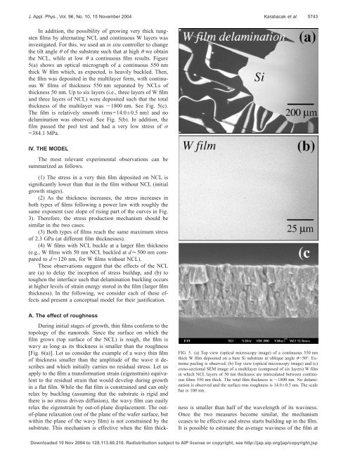
In addition, the possibility of grow<strong>in</strong>g very thick <strong>tungsten</strong><br />
<strong>films</strong> by alternat<strong>in</strong>g NCL and cont<strong>in</strong>uous W layers was<br />
<strong>in</strong>vestigated. For this, we used an <strong>in</strong> situ controller to change<br />
the tilt angle of the substrate such that at high we obta<strong>in</strong><br />
the NCL, while at low a cont<strong>in</strong>uous film results. Figure<br />
5(a) shows an optical micrograph of a cont<strong>in</strong>uous 550 nm<br />
thick W film which, as expected, is heavily buckled. Then,<br />
the film was deposited <strong>in</strong> the multilayer form, with cont<strong>in</strong>uous<br />
W <strong>films</strong> of thickness 550 nm separated by NCLs of<br />
thickness 50 nm. Up to six layers (i.e., three layers of W film<br />
and three layers of NCL) were deposited such that the total<br />
thickness of the multilayer was 1800 nm. See Fig. 5(c).<br />
The film is relatively smooth rms=14.0±0.5 nm and no<br />
delam<strong>in</strong>ation was observed. See Fig. 5(b). In addition, the<br />
film passed the peel test and had a very low stress of <br />
=384.1 MPa.<br />
IV. THE MODEL<br />
The most relevant experimental observations can be<br />
summarized as follows.<br />
(1) The stress <strong>in</strong> a very th<strong>in</strong> film deposited on NCL is<br />
significantly lower than that <strong>in</strong> the film without NCL (<strong>in</strong>itial<br />
growth stages).<br />
(2) As the thickness <strong>in</strong>creases, the stress <strong>in</strong>creases <strong>in</strong><br />
both types of <strong>films</strong> follow<strong>in</strong>g a power law with roughly the<br />
same exponent (see slope of ris<strong>in</strong>g part of the curves <strong>in</strong> Fig.<br />
3). Therefore, the stress production mechanism should be<br />
similar <strong>in</strong> the two cases.<br />
(3) Both types of <strong>films</strong> reach the same maximum stress<br />
of 2.3 GPa (at different film thicknesses).<br />
(4) W <strong>films</strong> with NCL buckle at a larger film thickness<br />
(e.g., W <strong>films</strong> with 50 nm NCL buckled at d500 nm compared<br />
to d120 nm, for W <strong>films</strong> without NCL).<br />
These observations suggest that the effects of the NCL<br />
are (a) to delay the <strong>in</strong>ception of stress buildup, and (b) to<br />
toughen the <strong>in</strong>terface such that delam<strong>in</strong>ation buckl<strong>in</strong>g occurs<br />
at higher levels of stra<strong>in</strong> energy stored <strong>in</strong> the film (larger film<br />
thickness). In the follow<strong>in</strong>g, we consider each of these effects<br />
and present a conceptual model for their justification.<br />
A. The effect of roughness<br />
Dur<strong>in</strong>g <strong>in</strong>itial stages of growth, th<strong>in</strong> <strong>films</strong> conform to the<br />
topology of the nanorods. S<strong>in</strong>ce the surface on which the<br />
film grows (top surface of the NCL) is rough, the film is<br />
wavy as long as its thickness is smaller than the roughness<br />
[Fig. 6(a)]. Let us consider the example of a wavy th<strong>in</strong> film<br />
of thickness smaller than the amplitude of the wave it describes<br />
and which <strong>in</strong>itially carries no residual stress. Let us<br />
apply to the film a transformation stra<strong>in</strong> (eigenstra<strong>in</strong>) equivalent<br />
to the residual stra<strong>in</strong> that would develop dur<strong>in</strong>g growth<br />
<strong>in</strong> a flat film. While the flat film is constra<strong>in</strong>ed and can only<br />
relax by buckl<strong>in</strong>g (assum<strong>in</strong>g that the substrate is rigid and<br />
there is no stress driven diffusion), the wavy film can easily<br />
relax the eigenstra<strong>in</strong> by out-of-plane displacement. The outof-plane<br />
relaxation (out of the plane of the wafer surface, but<br />
with<strong>in</strong> the plane of the wavy film) is not constra<strong>in</strong>ed by the<br />
substrate. This mechanism is effective when the film thick-<br />
FIG. 5. (a) Top view (optical microscopy image) of a cont<strong>in</strong>uous 550 nm<br />
thick W film deposited on a bare Si substrate at oblique angle =50°. Extreme<br />
peel<strong>in</strong>g is observed. (b) Top view (optical microscopy image) and (c)<br />
cross-sectional SEM image of a multilayer (composed of six layers) Wfilm<br />
<strong>in</strong> which NCL layers of 50 nm thickness are <strong>in</strong>tercalated between cont<strong>in</strong>uous<br />
<strong>films</strong> 550 nm thick. The total film thickness is 1800 nm. No delam<strong>in</strong>ation<br />
is observed and the surface rms roughness is 14.0±0.5 nm. The scale<br />
bar is 100 nm.<br />
ness is smaller than half of the wavelength of its wav<strong>in</strong>ess.<br />
Once the two measures become similar, the mechanism<br />
ceases to be effective and stress starts build<strong>in</strong>g up <strong>in</strong> the film.<br />
It is possible to estimate the average wav<strong>in</strong>ess of the film at<br />
Downloaded 10 Nov 2004 to 128.113.60.210. Redistribution subject to AIP license or copyright, see http://jap.aip.org/jap/copyright.jsp