nanoscopy - attocube
nanoscopy - attocube
nanoscopy - attocube

Create successful ePaper yourself
Turn your PDF publications into a flip-book with our unique Google optimized e-Paper software.
For many years, <strong>attocube</strong> systems has been pioneering cryogenic confocal microscopy. With the introduction of the<br />
attoCFM series of confocal microscopes almost a decade ago, the optical investigation of single quantum devices on the<br />
sub-micron scale at low temperature suddenly became available as a standard tool for scientists worldwide. Now once<br />
again, the attoCFM-MC is redefining the state-of-the-art for low temperature confocal microscopy.<br />
To improve the image quality in high resolution microscopy, confocal<br />
microscopes are often used at cryogenic temperatures. At these conditions,<br />
a combination of high resolution power, clear optical spectra,<br />
and reduced thermal noise can be achieved.<br />
Spectral lines become sharper as thermal broadening is typically<br />
reduced at cryogenic temperature. Optical signals become stronger as<br />
quantum efficiency improves because of reduced scattering and nonradiative<br />
recombinations.<br />
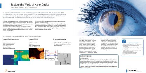
Cryogenic Photoluminescence<br />
- quantum dot luminescence<br />
- color centers in diamond<br />
- photonic crystals<br />
- single molecules<br />
- device electroluminescence<br />
Explore the World of Nano-Optics<br />
multichannel cryogenic confocal microscopes<br />
WIDE RANGE OF CRYOGENIC CONFOCAL MICROSCOPY APPLICATIONS<br />
pioneers of precision<br />
- carbon nanotubes<br />
- Graphene<br />
- high Tc superconductors<br />
- semiconductor nanowires<br />
For many optical microscopy applications cryogenic temperatures are<br />
therefore inevitably required.<br />
These advantages are beneficial particularly for high resolution optical<br />
spectroscopy of semiconductor structures or single molecule detection.<br />
Thus, investigation of the emitted optical energy of the sample due to<br />
changes in the surrounding material, applied voltages, or the deposited<br />
optical energy becomes feasible.<br />
Cryogenic RAMAN Cryogenic Lithography<br />
Detector cts<br />
3000<br />
2000<br />
1000<br />
Graphene at 4.2 K<br />
Monolayer<br />
Bilayer<br />
Edge<br />
D band<br />
G band<br />
0<br />
1000 1500 2000<br />
Raman shift (cm<br />
2500 3000<br />
-1 )<br />
- multiwavelength cryogenic lithography<br />
for deterministic quantum information<br />
device fabrication<br />
2D band<br />
With its all-new optical head, the<br />
attoCFM-MC opens the door to a whole<br />
new plethora of application fields<br />
through its easy-to-use and modular<br />
design. Whether your are working at<br />
the forefront of science in the fields of<br />
photoluminescence / fluorescence of<br />
e.g. semiconducting nanostructures<br />
(quantum dots, nano wires, photonics<br />
crystals, NV colour centers,…), Raman<br />
spectroscopy (e.g. on graphene, carbon<br />
CUSTOMER FEEDBACK<br />
nanotubes, high-Tc superconductors)<br />
or device fabrication for quantum<br />
optics (such as deterministic in-situ<br />
lithography on self-assembled quantum<br />
dots to form strongly coupled cavities),<br />
the attoCFM is the tool of choice to<br />
accelerate your research and and to<br />
achieve what matters most: creating<br />
scientific impact.<br />
Dr. Gervasi Herranz:<br />
The installation of the attoCFM has been carried out in spring 2011 and the system has<br />
been giving full satisfaction since its installation. We are very pleased with all the technical<br />
information and assistance provided during as well as after the purchase. Since the<br />
installation the system complies with all the specfications and requirements.<br />
(Magnetic Materials and Functional Oxides Group at the Institut de Ciència de Materials<br />
de Barcelona in Spain).<br />
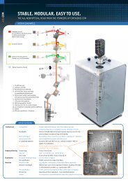
KEY FEATURES AND BENEFITS<br />
+ outstanding stability for long-term experiments<br />
+ modular design and exchangeable optical<br />
components<br />
+ compatible with mK temperatures and high magnetic<br />
fields (> 15 T)<br />
+ complete cryogen-free systems available as toploading<br />
or table-top setups<br />
+ diffraction limited spatial resolution<br />
+ 5 x 5 x 5 mm 3 positioning range at<br />
low temperature<br />
nanoSCOPY<br />
Scanning Probe Microscopes for Extreme Environments