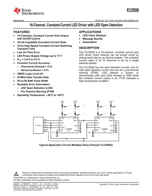
16-Channel, Constant-Current LED Driver with LED Open Detection
16-Channel, Constant-Current LED Driver with LED Open Detection
16-Channel, Constant-Current LED Driver with LED Open Detection

You also want an ePaper? Increase the reach of your titles
YUMPU automatically turns print PDFs into web optimized ePapers that Google loves.
1<br />
TLC5928<br />
www.ti.com ................................................................................................................................................. SBVS120A–JULY 2008–REVISED SEPTEMBER 2008<br />
<strong>16</strong>-<strong>Channel</strong>, <strong>Constant</strong>-<strong>Current</strong> <strong>LED</strong> <strong>Driver</strong> <strong>with</strong> <strong>LED</strong> <strong>Open</strong> <strong>Detection</strong><br />
1FEATURES<br />
APPLICATIONS<br />
23• <strong>16</strong> <strong>Channel</strong>s, <strong>Constant</strong> <strong>Current</strong> Sink Output • <strong>LED</strong> Video Displays<br />
<strong>with</strong> On/Off Control • Message Boards<br />
• 35-mA Capability (<strong>Constant</strong> <strong>Current</strong> Sink)<br />
• Illumination<br />
• 10-ns High-Speed <strong>Constant</strong> <strong>Current</strong> Switching<br />
Transient Time<br />
DESCRIPTION<br />
• Low On-Time Error<br />
The TLC5928 is a <strong>16</strong>-channel, constant current sink<br />
• <strong>LED</strong> Power-Supply Voltage up to 17 V<br />
<strong>LED</strong> driver. Each channel can be turned on/off by<br />
writing serial data to an internal register. The constant<br />
• V CC = 3.0 V to 5.5 V current value of all <strong>16</strong> channels is set by a single<br />
• <strong>Constant</strong> <strong>Current</strong> Accuracy: external resistor.<br />
– <strong>Channel</strong>-to-<strong>Channel</strong> = ±1% The TLC5928 has two error detection circuits: one for<br />
– Device-to-Device = ±1%<br />
<strong>LED</strong> open detection (LOD) and one for a pre-thermal<br />
• CMOS Logic Level I/O<br />
warning (PTW). LOD detects a broken or<br />
disconnected <strong>LED</strong> and <strong>LED</strong>s shorted to GND while<br />
• 35-MHz Data Transfer Rate the constant current output is on. PTW indicates a<br />
• 20-ns BLANK Pulse Width high temperature condition.<br />
• Readable Error Information:<br />
– <strong>LED</strong> <strong>Open</strong> <strong>Detection</strong> (LOD)<br />
– Pre-Thermal Warning (PTW)<br />
• Operating Temperature: –40°C to +85°C<br />
V<strong>LED</strong><br />
V<strong>LED</strong><br />
V<strong>LED</strong><br />
V<strong>LED</strong><br />
<br />
<br />
<br />
<br />
<br />
<br />
Controller<br />
DATA<br />
SCLK<br />
LAT<br />
BLANK<br />
ERROR<br />
READ<br />
OUT0<br />
SIN<br />
SCLK<br />
LAT<br />
BLANK<br />
IREF<br />
<br />
TLC5928<br />
IC1<br />
OUT15<br />
SOUT<br />
VCC<br />
GND<br />
VCC<br />
OUT0<br />
SIN<br />
SCLK<br />
LAT<br />
BLANK<br />
IREF<br />
<br />
TLC5928<br />
ICn<br />
OUT15<br />
SOUT<br />
VCC<br />
GND<br />
VCC<br />
R IREF<br />
R IREF<br />
3<br />
Typical Application Circuit (Multiple Daisy-Chained TLC5928s)<br />
Please be aware that an important notice concerning availability, standard warranty, and use in critical applications of Texas<br />
Instruments semiconductor products and disclaimers thereto appears at the end of this data sheet.<br />
2PowerPAD is a trademark of Texas Instruments, Inc.<br />
3All other trademarks are the property of their respective owners.<br />
UNLESS OTHERWISE NOTED this document contains Copyright © 2008, Texas Instruments Incorporated<br />
PRODUCTION DATA information current as of publication date.<br />
Products conform to specifications per the terms of Texas<br />
Instruments standard warranty. Production processing does not<br />
necessarily include testing of all parameters.
TLC5928<br />
SBVS120A–JULY 2008–REVISED SEPTEMBER 2008 ................................................................................................................................................. www.ti.com<br />
This integrated circuit can be damaged by ESD. Texas Instruments recommends that all integrated circuits be handled <strong>with</strong><br />
appropriate precautions. Failure to observe proper handling and installation procedures can cause damage.<br />
ESD damage can range from subtle performance degradation to complete device failure. Precision integrated circuits may be more<br />
susceptible to damage because very small parametric changes could cause the device not to meet its published specifications.<br />
PACKAGE/ORDERING INFORMATION (1)<br />
PRODUCT PACKAGE-LEAD ORDERING NUMBER TRANSPORT MEDIA, QUANTITY<br />
TLC5928<br />
TLC5928<br />
TLC5928<br />
SO-24<br />
TSSOP-24<br />
HTSSOP-24 PowerPAD<br />
TLC5928DBQR Tape and Reel, 2500<br />
TLC5928DBQ Tube, 50<br />
TLC5928PWR Tape and Reel, 2000<br />
TLC5928PW Tube, 60<br />
TLC5928PWPR Tape and Reel, 2000<br />
TLC5928PWP Tube, 60<br />
TLC5928RGER Tape and Reel, 3000<br />
TLC5928 QFN-24 (2) TLC5928RGE Tape and Reel, 250<br />
(1) For the most current package and ordering information see the Package Option Addendum at the end of this document, or see the TI<br />
web site at www.ti.com.<br />
(2) Shaded cells indicate product preview device.<br />
ABSOLUTE MAXIMUM RATINGS (1)(2)<br />
Over operating free-air temperature range, unless otherwise noted.<br />
DISSIPATION RATINGS<br />
PARAMETER TLC5928 UNIT<br />
V CC Supply voltage: V CC –0.3 to +6.0 V<br />
I OUT Output current (dc) OUT0 to OUT15 40 mA<br />
V IN Input voltage range SIN, SCLK, LAT, BLANK, IREF –0.3 to V CC + 0.3 V<br />
V OUT<br />
Output voltage range<br />
SOUT –0.3 to V CC + 0.3 V<br />
OUT0 to OUT15 –0.3 to +18 V<br />
T J(MAX) Operating junction temperature +150 °C<br />
T STG Storage temperature range –55 to +150 °C<br />
ESD rating<br />
Human body model (HBM) 2 kV<br />
Charged device model (CDM) 500 V<br />
(1) Stresses above these ratings may cause permanent damage. Exposure to absolute maximum conditions for extended periods may<br />
degrade device reliability. These are stress ratings only, and functional operation of the device at these or any other conditions beyond<br />
those specified is not supported.<br />
(2) All voltage values are <strong>with</strong> respect to network ground terminal.<br />
OPERATING FACTOR T A < +25°C T A = +70°C T A = +85°C<br />
PACKAGE ABOVE T A = +25°C POWER RATING POWER RATING POWER RATING<br />
SO-24 14.3 mW/°C 1782 mW 1140 mW 927 mW<br />
TSSOP-24 9.6 mW/°C 1194 mW 764 mW 621 mW<br />
HTSSOP-24 (1) 28.9 mW/°C 3611 mW 2311 mW 1878 mW<br />
QFN-24 (2) 24.8 mW/°C 3106 mW 1988 mW <strong>16</strong>15 mW<br />
(1) With PowerPAD soldered onto copper area on printed circuit board (PCB); 2 oz. copper. For more information, see SLMA002 (available<br />
for download at www.ti.com).<br />
(2) The package thermal impedance is calculated in accordance <strong>with</strong> JESD51-5.<br />
2 Submit Documentation Feedback Copyright © 2008, Texas Instruments Incorporated<br />
Product Folder Link(s): TLC5928
TLC5928<br />
www.ti.com ................................................................................................................................................. SBVS120A–JULY 2008–REVISED SEPTEMBER 2008<br />
RECOMMENDED OPERATING CONDITIONS<br />
At T A = –40°C to +85°C, unless otherwise noted.<br />
DC Characteristics: V CC = 3 V to 5.5 V<br />
TLC5928<br />
PARAMETER TEST CONDITIONS MIN NOM MAX UNIT<br />
V CC Supply voltage 3.0 5.5 V<br />
V O Voltage applied to output OUT0 to OUT15 17 V<br />
V IH High-level input voltage 0.7 × V CC V CC V<br />
V IL Low-level input voltage GND 0.3 × V CC V<br />
I OH High-level output current SOUT –1 mA<br />
I OL Low-level output current SOUT 1 mA<br />
I OLC <strong>Constant</strong> output sink current OUT0 to OUT15 2 35 mA<br />
T A Operating free-air temperature range –40 +85 °C<br />
T J Operating junction temperature range –40 +125 °C<br />
AC Characteristics: V CC = 3 V to 5.5 V<br />
f CLK (SCLK) Data shift clock frequency SCLK 35 MHz<br />
T WH0 SCLK 10 ns<br />
T WL0 SCLK 10 ns<br />
T WH1 Pulse duration LAT 20 ns<br />
T WH2 BLANK 20 ns<br />
T WL2 BLANK 20 ns<br />
T SU0 SIN–SCLK↑ 4 ns<br />
Setup time<br />
T SU1 LAT↑–SCLK↑ 100 ns<br />
T H0 SIN–SCLK↑ 3 ns<br />
Hold time<br />
T H1 LAT↑–SCLK↑ 10 ns<br />
Copyright © 2008, Texas Instruments Incorporated Submit Documentation Feedback 3<br />
Product Folder Link(s): TLC5928
TLC5928<br />
SBVS120A–JULY 2008–REVISED SEPTEMBER 2008 ................................................................................................................................................. www.ti.com<br />
ELECTRICAL CHARACTERISTICS<br />
At V CC = 3.0 V to 5.5 V and T A = –40°C to +85°C. Typical values at V CC = 3.3 V and T A = +25°C, unless otherwise noted.<br />
(%) =<br />
I OUTn<br />
1<br />
(I OUT0 + I OUT1 + ... + I OUT14 + I OUT15)<br />
<strong>16</strong><br />
.<br />
(2) The deviation of the OUT0–OUT15 constant current average from the ideal constant current value.<br />
Deviation is calculated by the following formula:<br />
(%) =<br />
I<br />
OUT(IDEAL)<br />
(I + I + ... I + I )<br />
OUT0 OUT1 OUT14 OUT15<br />
= 42 <br />
1.20<br />
<strong>16</strong><br />
Ideal Output <strong>Current</strong><br />
100<br />
(Ideal Output <strong>Current</strong>)<br />
100<br />
TLC5928<br />
PARAMETER TEST CONDITIONS MIN TYP MAX UNIT<br />
V OH High-level output voltage I OH = –1 mA at SOUT V CC – 0.4 V CC V<br />
V OL Low-level output voltage I OL = 1 mA at SOUT 0 0.4 V<br />
I IN Input current V IN = V CC or GND at SIN, SCLK, LAT, and BLANK –1 1 µA<br />
SIN/SCLK/LAT = low, BLANK = high, V OUTn = 1 V,<br />
I CC1 1 2 mA<br />
R IREF = 27 kΩ<br />
SIN/SCLK/LAT = low, BLANK = high, V OUTn = 1 V,<br />
I CC2 4.5 8 mA<br />
R IREF = 3 kΩ<br />
Supply current (V CC )<br />
SIN/SCLK/LAT/BLANK = low, V OUTn = 1 V,<br />
I CC3 7 18 mA<br />
R IREF = 3 kΩ<br />
SIN/SCLK/LAT/BLANK = low, V OUTn = 1 V,<br />
I CC4 <strong>16</strong> 40 mA<br />
R IREF = 1.5 kΩ<br />
All OUTn = ON, V OUTn = V OUTfix = 1 V, R IREF = 1.5 kΩ<br />
I OLC <strong>Constant</strong> output current 31 34 37 mA<br />
(see Figure 6), at OUT0 to OUT15<br />
All OUTn for constant current driver, all outputs off<br />
I OLKG Output leakage current BLANK = high, V OUTn = V OUTfix = 17 V, R IREF = 1.5 kΩ 0.1 µA<br />
(see Figure 6), at OUT0 to OUT15<br />
<strong>Constant</strong> current error<br />
All OUTn = ON, V OUTn = V OUTfix = 1 V, R IREF = 1.5 kΩ<br />
ΔI OLC ±1 ±3 %<br />
(channel-to-channel) (1)<br />
at OUT0 to OUT15<br />
<strong>Constant</strong> current error<br />
All OUTn = ON, V OUTn = V OUTfix = 1 V, R IREF = 1.5 kΩ<br />
ΔI OLC1 ±1 ±6 %<br />
(device-to-device) (2)<br />
at OUT0 to OUT15<br />
All OUTn = ON, V OUTn = V OUTfix = 1 V, R IREF = 1.5 kΩ<br />
ΔI OLC2 Line regulation (3) ±0.5 ±1 %/V<br />
at OUT0 to OUT15<br />
All OUTn = ON, V OUTn = 1 V to 3V, V OUTfix = 1 V,<br />
ΔI OLC3 Load regulation (4) ±1 ±3 %/V<br />
R IREF = 1.5 kΩ, at OUT0 to OUT15<br />
T (PTW) Pre-thermal warning threshold Junction temperature (5) +125 +138 +150 °C<br />
V LOD <strong>LED</strong> open detection threshold All OUTn = ON 0.25 0.30 0.35 V<br />
V IREF Reference voltage output R IREF = 1.5 kΩ 1.<strong>16</strong> 1.20 1.24 V<br />
(1) The deviation of each output from the average of OUT0–OUT15 constant current. Deviation is calculated by the formula:<br />
Ideal current is calculated by the formula:<br />
100<br />
(3) Line regulation is calculated by this equation:<br />
(%/V) =<br />
(IOUTn at V CC = 5.5 V) (IOUTn at V CC = 3.0 V)<br />
<br />
R IREF<br />
(IOUTn<br />
at V CC = 3.0 V)<br />
5.5 V 3 V<br />
(4) Load regulation is calculated by the equation:<br />
(%/V) =<br />
(IOUTn at V<br />
OUTn<br />
= 3 V) (IOUTn at V<br />
OUTn<br />
= 1 V)<br />
(IOUTn<br />
at V<br />
OUTn<br />
= 1 V)<br />
(5) Not tested. Specified by design.<br />
<br />
100<br />
3 V 1 V<br />
4 Submit Documentation Feedback Copyright © 2008, Texas Instruments Incorporated<br />
Product Folder Link(s): TLC5928
TLC5928<br />
www.ti.com ................................................................................................................................................. SBVS120A–JULY 2008–REVISED SEPTEMBER 2008<br />
SWITCHING CHARACTERISTICS<br />
At V CC = 3.0 V to 5.5 V, T A = –40°C to +85°C, C L = 15 pF, R L = 130 Ω, R IREF = 1.5 kΩ, and V <strong>LED</strong> = 5.5 V. Typical values at<br />
V CC = 3.3 V and T A = +25°C, unless otherwise noted.<br />
TLC5928<br />
PARAMETER TEST CONDITIONS MIN TYP MAX UNIT<br />
t R0 SOUT (see Figure 5) 5 15 ns<br />
Rise time<br />
t R1 OUTn (see Figure 4) 10 30 ns<br />
t F0 SOUT (see Figure 5) 5 15 ns<br />
Fall time<br />
t F1 OUTn (see Figure 4) 10 30 ns<br />
t D0 SCLK↑ to SOUT 8 20 ns<br />
LAT↑ or BLANK↓ to OUTn sink current on<br />
t D1 12 30 ns<br />
Propagation delay time (see Figure 10)<br />
LAT↑ or BLANK↑ to OUTn sink current off<br />
t D2 12 30 ns<br />
(see Figure 10)<br />
On/off latch data = all '1', 20 ns BLANK low level<br />
t ON_ERR Output on-time error (1) –8 +8 ns<br />
one-shot pulse input (see Figure 4)<br />
(1) Output on-time error (t ON_ERR ) is calculated by the formula: t ON_ERR (ns) = t OUT_ON – BLANK low level one-shot pulse width (T WL2 ).<br />
t OUT_ON indicates the actual on-time of the constant current driver.<br />
FUNCTIONAL BLOCK DIAGRAM<br />
VCC<br />
VCC<br />
SIN<br />
SCLK<br />
LAT<br />
LSB<br />
On/Off Control Shift Register<br />
(1 Bit x <strong>16</strong> <strong>Channel</strong>s)<br />
MSB<br />
0 15<br />
<strong>16</strong><br />
LSB<br />
On/Off Control Data Latch<br />
(1 Bit x <strong>16</strong> <strong>Channel</strong>s)<br />
MSB<br />
<strong>16</strong><br />
SOUT<br />
BLANK<br />
0 15<br />
<strong>16</strong><br />
SID Latch<br />
IREF<br />
<strong>16</strong>-<strong>Channel</strong> <strong>Constant</strong> <strong>Current</strong> Sink <strong>Driver</strong><br />
Thermal<br />
<strong>Detection</strong><br />
<strong>16</strong><br />
GND<br />
<strong>16</strong>-<strong>Channel</strong> <strong>LED</strong> <strong>Open</strong> <strong>Detection</strong><br />
GND<br />
<br />
OUT0 OUT1 OUT14 OUT15<br />
Copyright © 2008, Texas Instruments Incorporated Submit Documentation Feedback 5<br />
Product Folder Link(s): TLC5928
TLC5928<br />
SBVS120A–JULY 2008–REVISED SEPTEMBER 2008 ................................................................................................................................................. www.ti.com<br />
DEVICE INFORMATION<br />
SO-24 AND TSSOP-24<br />
DBQ AND PW PACKAGES<br />
(TOP VIEW)<br />
HTSSOP-24 PowerPAD<br />
PWP PACKAGE<br />
(TOP VIEW)<br />
GND<br />
1<br />
24<br />
VCC<br />
GND<br />
1<br />
24<br />
VCC<br />
SIN<br />
2<br />
23<br />
IREF<br />
SIN<br />
2<br />
23<br />
IREF<br />
SCLK<br />
3<br />
22<br />
SOUT<br />
SCLK<br />
3<br />
22<br />
SOUT<br />
LAT<br />
4<br />
21<br />
BLANK<br />
LAT<br />
4<br />
21<br />
BLANK<br />
OUT0<br />
5<br />
20<br />
OUT15<br />
OUT0<br />
5<br />
20<br />
OUT15<br />
OUT1<br />
OUT2<br />
6<br />
7<br />
TLC5928<br />
19<br />
18<br />
OUT14<br />
OUT13<br />
OUT1<br />
OUT2<br />
6<br />
7<br />
Thermal Pad<br />
(Bottom Side)<br />
TLC5928<br />
19<br />
18<br />
OUT14<br />
OUT13<br />
OUT3<br />
8<br />
17<br />
OUT12<br />
OUT3<br />
8<br />
17<br />
OUT12<br />
OUT4<br />
9<br />
<strong>16</strong><br />
OUT11<br />
OUT4<br />
9<br />
<strong>16</strong><br />
OUT11<br />
OUT5<br />
10<br />
15<br />
OUT10<br />
OUT5<br />
10<br />
15<br />
OUT10<br />
OUT6<br />
11<br />
14<br />
OUT9<br />
OUT6<br />
11<br />
14<br />
OUT9<br />
OUT7<br />
12<br />
13<br />
OUT8<br />
OUT7<br />
12<br />
13<br />
OUT8<br />
QFN-24 (1)<br />
RGE PACKAGE<br />
(TOP VIEW)<br />
SCLK<br />
SIN<br />
GND<br />
VCC<br />
IREF<br />
SOUT<br />
24<br />
23<br />
22<br />
21<br />
20<br />
19<br />
LAT<br />
1<br />
18<br />
BLANK<br />
OUT0<br />
2<br />
17<br />
OUT15<br />
OUT1<br />
OUT2<br />
3<br />
4<br />
Thermal Pad<br />
(Bottom Side)<br />
TLC5928<br />
<strong>16</strong><br />
15<br />
OUT14<br />
OUT13<br />
OUT3<br />
5<br />
14<br />
OUT12<br />
OUT4<br />
6<br />
13<br />
OUT11<br />
OUT5 7<br />
OUT6 8<br />
OUT7 9<br />
OUT8 10<br />
OUT9 11<br />
OUT10 12<br />
NOTE: Thermal pad is not connected to GND internally. The thermal pad must be connected to GND via the PCB pattern.<br />
(1) Product preview device.<br />
6 Submit Documentation Feedback Copyright © 2008, Texas Instruments Incorporated<br />
Product Folder Link(s): TLC5928
TLC5928<br />
www.ti.com ................................................................................................................................................. SBVS120A–JULY 2008–REVISED SEPTEMBER 2008<br />
TERMINAL<br />
TERMINAL FUNCTIONS<br />
DBQ/PW/<br />
NAME PWP RGE I/O DESCRIPTION<br />
SIN 2 23 I<br />
Serial data input for driver on/off control. When SIN = high level, data '1' are written into LSB<br />
of the on/off control shift register at the rising edge of SCLK.<br />
Serial data shift clock. Schmitt buffer input. All data in the on/off control shift register are<br />
SCLK 3 24 I shifted toward the MSB by 1-bit synchronization of SCLK. A rising edge on SCLK is allowed<br />
100 ns after a rising edge of LAT.<br />
Edge triggered latch. The data in the on/off control data shift register are transferred to the<br />
on/off control data latch at this rising edge. At the same time, the data in the on/off control shift<br />
LAT 4 1 I register are replaced <strong>with</strong> <strong>LED</strong> open detection (LOD) and pre-thermal warning (PTW) data.<br />
LAT must be toggled only once after the shift data are updated to avoid the on/off control latch<br />
data being replaced <strong>with</strong> LOD and PTW data in the shift register.<br />
BLANK 21 18 I<br />
Blank, all outputs. When BLANK = high level, all constant current outputs (OUT0–OUT15) are<br />
forced off. When BLANK = low level, all constant current outputs are controlled by the on/off<br />
control data in the data latch. LOD and PTW data are latched into the SID data latch at the<br />
rising edge of BLANK and are present at the output of the SID data latch when BLANK is low.<br />
<strong>Constant</strong> current value setting, OUT0–OUT15 sink constant current is set to desired value by<br />
IREF 23 20 I/O connection to an external resistor between IREF and GND.<br />
SOUT 22 19 O<br />
OUT0 5 2 O<br />
OUT1 6 3 O <strong>Constant</strong> current output<br />
OUT2 7 4 O <strong>Constant</strong> current output<br />
OUT3 8 5 O <strong>Constant</strong> current output<br />
OUT4 9 6 O <strong>Constant</strong> current output<br />
OUT5 10 7 O <strong>Constant</strong> current output<br />
OUT6 11 8 O <strong>Constant</strong> current output<br />
OUT7 12 9 O <strong>Constant</strong> current output<br />
OUT8 13 10 O <strong>Constant</strong> current output<br />
OUT9 14 11 O <strong>Constant</strong> current output<br />
OUT10 15 12 O <strong>Constant</strong> current output<br />
OUT11 <strong>16</strong> 13 O <strong>Constant</strong> current output<br />
OUT12 17 14 O <strong>Constant</strong> current output<br />
OUT13 18 15 O <strong>Constant</strong> current output<br />
OUT14 19 <strong>16</strong> O <strong>Constant</strong> current output<br />
OUT15 20 17 O <strong>Constant</strong> current output<br />
VCC 24 21 — Power-supply voltage<br />
GND 1 22 — Power ground<br />
Serial data output. This output is connected to the MSB of the on/off data shift register. SOUT<br />
data changes at the rising edge of SCLK.<br />
<strong>Constant</strong> current output. Each output can be tied together <strong>with</strong> others to increase the constant<br />
current. Different voltages can be applied to each output.<br />
Copyright © 2008, Texas Instruments Incorporated Submit Documentation Feedback 7<br />
Product Folder Link(s): TLC5928
TLC5928<br />
SBVS120A–JULY 2008–REVISED SEPTEMBER 2008 ................................................................................................................................................. www.ti.com<br />
PARAMETER MEASUREMENT INFORMATION<br />
PIN EQUIVALENT INPUT AND OUTPUT SCHEMATIC DIAGRAMS<br />
VCC<br />
VCC<br />
INPUT<br />
SOUT<br />
GND<br />
Figure 1. SIN, SCLK, LAT, BLANK<br />
Figure 2. SOUT<br />
GND<br />
OUTn<br />
GND<br />
Figure 3. OUT0 Through OUT15<br />
TEST CIRCUITS<br />
V CC<br />
R IREF<br />
IREF<br />
VCC<br />
GND<br />
OUTn<br />
R L<br />
C L<br />
(1)<br />
V <strong>LED</strong> V CC<br />
VCC<br />
GND<br />
SOUT<br />
C L<br />
(1)<br />
(1) C L includes measurement probe and jig capacitance. (1) C L includes measurement probe and jig capacitance.<br />
Figure 4. Rise Time and Fall Time Test Circuit for OUTn<br />
Figure 5. Rise Time and Fall Time Test Circuit for SOUT<br />
VCC<br />
OUT0<br />
V CC<br />
R IREF<br />
VOUT FIX<br />
VOUTn<br />
IREF<br />
OUTn<br />
GND<br />
OUT15<br />
Figure 6. <strong>Constant</strong> <strong>Current</strong> Test Circuit for OUTn<br />
8 Submit Documentation Feedback Copyright © 2008, Texas Instruments Incorporated<br />
Product Folder Link(s): TLC5928
TLC5928<br />
www.ti.com ................................................................................................................................................. SBVS120A–JULY 2008–REVISED SEPTEMBER 2008<br />
TIMING DIAGRAMS<br />
T WH0, T WL0, TWH1, T WH2, T WL2:<br />
V CC<br />
INPUT (1)<br />
50%<br />
GND<br />
T WH<br />
T WL<br />
T , T , T , T :<br />
SU0 SU1 H0 H1<br />
CLOCK<br />
INPUT (1)<br />
50%<br />
GND<br />
T SU T H<br />
V CC<br />
V CC<br />
DATA/CONTROL<br />
INPUT (1)<br />
50%<br />
(1) Input pulse rise and fall time is 1 ns to 3 ns.<br />
Figure 7. Input Timing<br />
GND<br />
t , t , t , t , t , t , t :<br />
R0 R1 F0 F1 D0 D1 D2<br />
V CC<br />
INPUT (1) 50%<br />
GND<br />
t D<br />
90%<br />
VOH<br />
or VOUTn<br />
OUTPUT<br />
50%<br />
10%<br />
(1) Input pulse rise and fall time is 1 ns to 3 ns.<br />
Figure 8. Output Timing<br />
tR<br />
or tF<br />
VOL<br />
or VOUTn<br />
Copyright © 2008, Texas Instruments Incorporated Submit Documentation Feedback 9<br />
Product Folder Link(s): TLC5928
TLC5928<br />
SBVS120A–JULY 2008–REVISED SEPTEMBER 2008 ................................................................................................................................................. www.ti.com<br />
SIN<br />
DATA<br />
0A<br />
DATA<br />
15B<br />
DATA<br />
14B<br />
DATA<br />
13B<br />
DATA<br />
12B<br />
DATA<br />
11B<br />
DATA<br />
3B<br />
DATA<br />
2B<br />
DATA<br />
1B<br />
DATA<br />
0B<br />
DATA<br />
15C<br />
DATA<br />
14C<br />
DATA<br />
13C<br />
DATA<br />
12C<br />
DATA<br />
11C<br />
DATA<br />
10C<br />
T SU0<br />
T H0<br />
T WL0<br />
SCLK<br />
T WH0<br />
T H1<br />
T WH1<br />
1 2 3 4 5 13 14 15 <strong>16</strong><br />
1 2 3 4 5 6<br />
T SU1<br />
LAT<br />
Shift Register<br />
LSB Data (Internal)<br />
DATA<br />
0A<br />
LOD<br />
0<br />
DATA<br />
15B<br />
DATA<br />
14B<br />
DATA<br />
13B<br />
DATA<br />
12B<br />
DATA<br />
3B<br />
DATA<br />
2B<br />
DATA<br />
1B<br />
DATA<br />
0B<br />
LOD 0A or PTW_A<br />
DATA<br />
15C<br />
DATA<br />
14C<br />
DATA<br />
13C<br />
DATA<br />
12C<br />
DATA<br />
11C<br />
Shift Register<br />
LSB+1 Data (Internal)<br />
DATA<br />
1A<br />
LOD<br />
1<br />
LOD<br />
0<br />
DATA<br />
15B<br />
DATA<br />
14B<br />
DATA<br />
13B<br />
DATA<br />
4B<br />
DATA<br />
3B<br />
DATA<br />
2B<br />
LOD 1A or PTW_A<br />
LOD<br />
0A<br />
DATA<br />
15C<br />
DATA<br />
14C<br />
DATA<br />
13C<br />
DATA<br />
12C<br />
Shift Register<br />
MSB-1 Data (Internal)<br />
DATA<br />
14A<br />
LOD<br />
14<br />
LOD<br />
13<br />
LOD<br />
12<br />
LOD<br />
11<br />
LOD<br />
10<br />
LOD<br />
1<br />
LOD<br />
0<br />
DATA<br />
15B<br />
LOD 14A or PTW_A<br />
LOD<br />
13A<br />
LOD<br />
12A<br />
LOD<br />
11A<br />
LOD<br />
10A<br />
LOD<br />
9A<br />
Shift Register<br />
MSB Data (Internal)<br />
DATA<br />
15A<br />
LOD<br />
15<br />
LOD<br />
14<br />
LOD<br />
13<br />
LOD<br />
12<br />
LOD<br />
11<br />
LOD<br />
2<br />
LOD<br />
1<br />
LOD<br />
0<br />
DATA<br />
15B<br />
LOD 15A or PTW_A<br />
LOD<br />
14A<br />
LOD<br />
13A<br />
LOD<br />
12A<br />
LOD<br />
11A<br />
LOD<br />
10A<br />
On/Off Control<br />
Latch Data (Internal)<br />
Previous Grayscale Latch Data<br />
Latest Grayscale Latch Data<br />
SOUT<br />
DATA<br />
15A<br />
LOD<br />
15<br />
LOD<br />
14<br />
LOD<br />
13<br />
LOD<br />
12<br />
LOD<br />
11<br />
LOD<br />
2<br />
LOD<br />
1<br />
LOD<br />
0<br />
DATA<br />
15B<br />
LOD 15A or PTW_A<br />
LOD<br />
14A<br />
LOD<br />
13A<br />
LOD<br />
12A<br />
LOD<br />
11A<br />
LOD<br />
10A<br />
t D0<br />
t /t R0 F0<br />
t WH2<br />
BLANK<br />
OUTn (1)<br />
OFF<br />
ON<br />
ON<br />
t D2<br />
ON<br />
OFF<br />
OUTn (2)<br />
OFF<br />
ON<br />
t D1<br />
ON<br />
t D1<br />
t WL2<br />
t OUTON<br />
tD2<br />
OFF<br />
OUTn (3)<br />
OUTn (4)<br />
OFF<br />
ON<br />
OFF<br />
ON<br />
t F1<br />
t D1<br />
OFF<br />
ON<br />
t R1<br />
OFF<br />
(1) On/off latched data are '1'.<br />
(2) On/off latched data are changed from '1' to '0' at the second LAT signal.<br />
(3) On/off latched data are changed from '0' to '1' at the second LAT signal.<br />
(4) On/off latched data are '0'.<br />
Figure 9. Timing Diagram<br />
10 Submit Documentation Feedback Copyright © 2008, Texas Instruments Incorporated<br />
Product Folder Link(s): TLC5928
TLC5928<br />
www.ti.com ................................................................................................................................................. SBVS120A–JULY 2008–REVISED SEPTEMBER 2008<br />
TYPICAL CHARACTERISTICS<br />
At V CC = 3.3 V and T A = +25°C, unless otherwise noted.<br />
100000<br />
REFERENCE RESISTOR<br />
vs OUTPUT CURRENT<br />
4000<br />
POWER DISSIPATION RATE<br />
vs FREE-AIR TEMPERATURE<br />
TLC5928PWP<br />
Reference Resistor ( )<br />
10000<br />
25200<br />
10080<br />
5040<br />
3360<br />
2520<br />
20<strong>16</strong><br />
<strong>16</strong>80<br />
Power Dissipation Rate (mW)<br />
3000<br />
2000<br />
1000<br />
TLC5928DBQ<br />
TLC5928RGE<br />
TLC5928PW<br />
1000<br />
1440<br />
0 5 10 15 20 25 30<br />
0<br />
40 20 0 20 40 60 80<br />
100<br />
Output <strong>Current</strong> (mA)<br />
Free-Air Temperature ( C)<br />
Figure 10. Figure 11.<br />
Output <strong>Current</strong> (mA)<br />
40<br />
35<br />
30<br />
25<br />
20<br />
15<br />
10<br />
5<br />
0<br />
T A = +25C<br />
I = 2 mA<br />
O<br />
OUTPUT CURRENT vs<br />
OUTPUT VOLTAGE<br />
0 0.5 1.0 1.5 2.0 2.5 3.0<br />
Output Voltage (V)<br />
I = 35 mA<br />
O<br />
I = 30 mA<br />
O<br />
I = 20 mA<br />
O<br />
I = 10 mA<br />
O<br />
I = 5 mA<br />
O<br />
Output <strong>Current</strong> (mA)<br />
40<br />
39<br />
38<br />
37<br />
36<br />
35<br />
34<br />
33<br />
32<br />
31<br />
I = 30 mA<br />
O<br />
OUTPUT CURRENT vs<br />
OUTPUT VOLTAGE<br />
30<br />
0 0.5 1.0 1.5 2.0 2.5 3.0<br />
Output Voltage (V)<br />
Figure 12. Figure 13.<br />
T A = 40C<br />
T A = +25C<br />
T A = +85C<br />
4<br />
3<br />
I = 35 mA<br />
O<br />
ΔI OLC vs AMBIENT TEMPERATURE<br />
4<br />
3<br />
T A = +25C<br />
ΔI OLC vs OUTPUT CURRENT<br />
2<br />
2<br />
I OLC (%)<br />
1<br />
0<br />
1<br />
I OLC (%)<br />
1<br />
0<br />
1<br />
2<br />
V CC = 3.3 V<br />
3<br />
V CC = 5 V<br />
4<br />
40 20 0 20 40 60 80 100<br />
Ambient Temperature ( C)<br />
2<br />
V CC = 3.3 V<br />
3<br />
V CC = 5 V<br />
4<br />
0 10 20 30 40<br />
Output <strong>Current</strong> (mA)<br />
Figure 14. Figure 15.<br />
Copyright © 2008, Texas Instruments Incorporated Submit Documentation Feedback 11<br />
Product Folder Link(s): TLC5928
TLC5928<br />
SBVS120A–JULY 2008–REVISED SEPTEMBER 2008 ................................................................................................................................................. www.ti.com<br />
At V CC = 3.3 V and T A = +25°C, unless otherwise noted.<br />
TYPICAL CHARACTERISTICS (continued)<br />
CONSTANT CURRENT OUTPUT<br />
VOLTAGE WAVEFORM<br />
CH1 (2 V/div)<br />
CH1-BLANK<br />
(20 ns)<br />
CH2 (2 V/div)<br />
CH2-OUT0<br />
(BLANK = 20 ns)<br />
CH3 (2 V/div)<br />
I OLC = 35 mA<br />
T<br />
A<br />
= +25C<br />
R L = 130 <br />
C<br />
L<br />
= 15 pF<br />
V<strong>LED</strong> = 5.5 V<br />
CH3-OUT15<br />
(BLANK = 20 ns)<br />
Time (12.5 ns/div)<br />
Figure <strong>16</strong>.<br />
12 Submit Documentation Feedback Copyright © 2008, Texas Instruments Incorporated<br />
Product Folder Link(s): TLC5928
TLC5928<br />
www.ti.com ................................................................................................................................................. SBVS120A–JULY 2008–REVISED SEPTEMBER 2008<br />
DETAI<strong>LED</strong> DESCRIPTION<br />
SETTING FOR THE CONSTANT SINK CURRENT VALUE<br />
The constant current values are determined by an external resistor (R IREF ) placed between IREF and GND. The<br />
resistor (R IREF ) value is calculated by Equation 1.<br />
V IREF (V)<br />
R IREF (k ) =<br />
42<br />
I<br />
OLC<br />
(mA)<br />
(1)<br />
Where:<br />
V IREF = the internal reference voltage on the IREF pin (typically 1.20 V)<br />
I OLC must be set in the range of 2 mA to 35 mA. The constant sink current characteristic for the external resistor<br />
value is shown in Figure 10. Table 1 describes the constant current output versus external resistor value.<br />
Table 1. <strong>Constant</strong> <strong>Current</strong> Output versus External Resistor Value<br />
I OLCMax (mA, Typical)<br />
CONSTANT CURRENT DRIVER ON/OFF CONTROL<br />
R IREF (kΩ)<br />
35 1.44<br />
30 1.68<br />
25 2.02<br />
20 2.52<br />
15 3.36<br />
10 5.04<br />
5 10.1<br />
2 25.2<br />
When BLANK is low, the corresponding output is turned on if the data in the on/off control data latch are '1' and<br />
remains off if the data are '0'. When BLANK is high, all outputs are forced off. This control is shown in Table 2.<br />
ON/OFF CONTROL LATCH DATA<br />
Table 2. On/Off Control Data Truth Table<br />
CONSTANT CURRENT OUTPUT STATUS<br />
0 Off<br />
1 On<br />
When the IC is initially powered on, the data in the on/off control shift register and data latch are not set to the<br />
respective default value. Therefore, the on/off control data must be written to the data latch before turning the<br />
constant current output on. BLANK should be at a high level when powered on because the constant current<br />
may be turned on as a result of random data in the on/off control latch.<br />
The on/off data corresponding to any unconnected OUTn outputs should be set to ‘0’ before turning on the<br />
remaining outputs. Otherwise, the supply current (I CC ) increases while the <strong>LED</strong>s are on.<br />
Copyright © 2008, Texas Instruments Incorporated Submit Documentation Feedback 13<br />
Product Folder Link(s): TLC5928
TLC5928<br />
SBVS120A–JULY 2008–REVISED SEPTEMBER 2008 ................................................................................................................................................. www.ti.com<br />
REGISTER CONFIGURATION<br />
The TLC5928 has an on/off control data shift register and data latch. Both the on/off control shift register and<br />
latch are <strong>16</strong> bits long and are used to turn on/off the constant current drivers. Figure 17 shows the shift register<br />
and latch configuration. The data at the SIN pin are shifted in to the LSB of the shift register at the rising edge of<br />
the SCLK pin; SOUT data change at the rising edge of SCLK. The timing diagram for data writing is shown in<br />
Figure 18. The driver on/off is controlled by the data in the on/off control data latch.<br />
The on/off data are latched into the data latch by a rising edge of LAT after the data are written into the on/off<br />
control shift register by SIN and SCLK. At the same time, the data in the on/off control shift register are replaced<br />
<strong>with</strong> <strong>LED</strong> open detection (LOD) and pre-thermal warning (PTW) data. Therefore, LAT must be input only once<br />
after the on/off data update to avoid the on/off control data latch being replaced <strong>with</strong> LOD and PTW data in the<br />
shift register. When the IC is initially powered on, the data in the on/off control shift register and latch are not set<br />
to the default values; on/off control data must be written to the on/off control data latch before turning the<br />
constant current output on. BLANK should be high when the IC is powered on because the constant current may<br />
be turned on at that time as a result of random values in the on/off data latch. All constant current outputs are<br />
forced off when BLANK is high.<br />
On/Off Control Shift Register (1 Bit <strong>16</strong> <strong>Channel</strong>s)<br />
MSB<br />
LSB<br />
SOUT<br />
15 14<br />
On/Off Data<br />
for<br />
OUT15<br />
On/Off Data<br />
for<br />
OUT14<br />
13 12 11<br />
4<br />
3 2<br />
On/Off Data<br />
for<br />
OUT13<br />
On/Off Data<br />
for<br />
OUT12<br />
<br />
On/Off Data<br />
for<br />
OUT3<br />
On/Off Data<br />
for<br />
OUT2<br />
1 0<br />
On/Off Data<br />
for<br />
OUT1<br />
On/Off Data<br />
for<br />
OUT0<br />
SIN<br />
SCLK<br />
<br />
MSB<br />
LSB<br />
15 14<br />
13 12 11<br />
4<br />
3 2<br />
1 0<br />
On/Off Data<br />
for<br />
OUT15<br />
On/Off Data<br />
for<br />
OUT14<br />
On/Off Data<br />
for<br />
OUT13<br />
On/Off Data<br />
for<br />
OUT12<br />
<br />
On/Off Data<br />
for<br />
OUT3<br />
On/Off Data<br />
for<br />
OUT2<br />
On/Off Data<br />
for<br />
OUT1<br />
On/Off Data<br />
for<br />
OUT0<br />
LAT<br />
On/Off Control Data Latch (1 Bit <strong>16</strong> <strong>Channel</strong>s)<br />
<strong>16</strong> Bits<br />
To <strong>Constant</strong> <strong>Current</strong> <strong>Driver</strong> Control Block<br />
Figure 17. On/Off Control Shift Register and Latch Configuration<br />
14 Submit Documentation Feedback Copyright © 2008, Texas Instruments Incorporated<br />
Product Folder Link(s): TLC5928
TLC5928<br />
www.ti.com ................................................................................................................................................. SBVS120A–JULY 2008–REVISED SEPTEMBER 2008<br />
SIN<br />
DATA<br />
0A<br />
DATA<br />
15B<br />
DATA<br />
14B<br />
DATA<br />
13B<br />
DATA<br />
12B<br />
DATA<br />
11B<br />
DATA<br />
3B<br />
DATA<br />
2B<br />
DATA<br />
1B<br />
DATA<br />
0B<br />
DATA<br />
15C<br />
DATA<br />
14C<br />
DATA<br />
13C<br />
DATA<br />
12C<br />
DATA<br />
11C<br />
DATA<br />
10C<br />
SCLK<br />
1 2 3 4 5 13 14 15 <strong>16</strong><br />
1 2 3 4 5 6<br />
LAT<br />
Shift Register<br />
LSB Data (Internal)<br />
DATA<br />
0A<br />
LOD<br />
0<br />
DATA<br />
15B<br />
DATA<br />
14B<br />
DATA<br />
13B<br />
DATA<br />
12B<br />
DATA<br />
3B<br />
DATA<br />
2B<br />
DATA<br />
1B<br />
DATA<br />
0B<br />
LOD 0A or PTW_A<br />
DATA<br />
15C<br />
DATA<br />
14C<br />
DATA<br />
13C<br />
DATA<br />
12C<br />
DATA<br />
11C<br />
Shift Register<br />
LSB+1 Data (Internal)<br />
DATA<br />
1A<br />
LOD<br />
1<br />
LOD<br />
0<br />
DATA<br />
15B<br />
DATA<br />
14B<br />
DATA<br />
13B<br />
DATA<br />
4B<br />
DATA<br />
3B<br />
DATA<br />
2B<br />
LOD 1A or PTW_A<br />
LOD<br />
0A<br />
DATA<br />
15C<br />
DATA<br />
14C<br />
DATA<br />
13C<br />
DATA<br />
12C<br />
<br />
<br />
<br />
Shift Register<br />
MSB1 Data(Internal)<br />
DATA<br />
14A<br />
LOD<br />
14<br />
LOD<br />
13<br />
LOD<br />
12<br />
LOD<br />
11<br />
LOD<br />
10<br />
LOD<br />
1<br />
LOD<br />
0<br />
DATA<br />
15B<br />
LOD 14A or PTW_A<br />
LOD<br />
13A<br />
LOD<br />
12A<br />
LOD<br />
11A<br />
LOD<br />
10A<br />
LOD<br />
9A<br />
Shift Register<br />
MSB Data(Internal)<br />
DATA<br />
1A<br />
LOD<br />
15<br />
LOD<br />
14<br />
LOD<br />
13<br />
LOD<br />
12<br />
LOD<br />
11<br />
LOD<br />
2<br />
LOD<br />
1<br />
LOD<br />
0<br />
DATA<br />
15B<br />
LOD 15A or PTW_A<br />
LOD<br />
14A<br />
LOD<br />
13A<br />
LOD<br />
12A<br />
LOD<br />
11A<br />
LOD<br />
10A<br />
On/Off Control<br />
Latch Data (Internal)<br />
Previous Grayscale Latch Data<br />
Latest Grayscale Latch Data<br />
SOUT<br />
DATA<br />
1A<br />
LOD<br />
15<br />
LOD<br />
14<br />
LOD<br />
13<br />
LOD<br />
12<br />
LOD<br />
11<br />
LOD<br />
2<br />
LOD<br />
1<br />
LOD<br />
0<br />
DATA<br />
15B<br />
LOD 15A or PTW_A<br />
LOD<br />
14A<br />
LOD<br />
13A<br />
LOD<br />
12A<br />
LOD<br />
11A<br />
LOD<br />
10A<br />
BLANK<br />
OUTn (1) OFF<br />
ON ON<br />
OFF<br />
OUTn (2)<br />
OFF<br />
ON<br />
ON<br />
OFF<br />
OUTn (3)<br />
OFF<br />
ON<br />
OFF<br />
ON<br />
OFF<br />
OUTn (4) OFF<br />
OFF<br />
ON<br />
(1) On/off latched data are '1'.<br />
(2) On/off latched data are changed from '1' to '0' at the second LAT signal.<br />
(3) On/off latched data are changed from '0' to '1' at the second LAT signal.<br />
(4) On/off latched data are '0'.<br />
OFF<br />
Figure 18. On/Off Control Operation<br />
Copyright © 2008, Texas Instruments Incorporated Submit Documentation Feedback 15<br />
Product Folder Link(s): TLC5928
TLC5928<br />
SBVS120A–JULY 2008–REVISED SEPTEMBER 2008 ................................................................................................................................................. www.ti.com<br />
<strong>LED</strong> OPEN DETECTION (LOD) AND PRE-THERMAL WARNING (PTW)<br />
The <strong>LED</strong> open detection (LOD) circuit checks the voltage of each active (that is, on) constant current sink output<br />
(OUT0 through OUT15) to detect open <strong>LED</strong>s and <strong>LED</strong>s shorted to GND while BLANK is low. The LOD bits in the<br />
status information data register (SID) are set to '1' if the voltage of the corresponding OUTn pin is less than the<br />
<strong>LED</strong> open detection threshold (V LOD = 0.3 V, typ). The status information data can be read from the SOUT pin.<br />
To avoid false detection of open <strong>LED</strong>s, the <strong>LED</strong> driver design must ensure that the constant-current sink output<br />
voltage is greater than 0.3 V when the outputs are on. Also, the output on-time must be 1 µs or greater to<br />
correctly read the valid LOD status.<br />
The PTW function indicates that the IC junction temperature is too high. The PTW bit in the SID data is set to '1'<br />
while the IC junction temperature exceeds the temperature threshold (T (PTW) = +138 °C, typ). If the IC junction<br />
temperature decreases below the temperature of T (PTW) , the SID data are set depending on the LOD function.<br />
The constant current outputs are not forced off during PTW conditions, so the controller should take appropriate<br />
action (such as reducing the duty cycle of effected channels).<br />
The LOD and PTW data are latched into the SID latch <strong>with</strong> the rising edge of BLANK and do not change until<br />
BLANK goes low. The SID data latched in the latch are transferred into the on/off shift register <strong>with</strong> a rising edge<br />
of LAT. SID can be shifted out from SOUT <strong>with</strong> rising edges of SCLK. The data in the on/off control shift register<br />
are replaced <strong>with</strong> the LOD and PTW data at the rising edge of LAT. Therefore, LAT should be input only once<br />
after the shift data are updated to avoid the on/off control data latch information from being replaced <strong>with</strong> LOD<br />
and PTW data in the shift register. A timing diagram for LOD, PTW, and SID is shown in Figure 19.<br />
BLANK<br />
OUTn<br />
LOD Circuit Data<br />
(Internal)<br />
OUTn ON<br />
GND<br />
No Error Information<br />
OUTn OFF<br />
LOD and PTW data are always copied into<br />
SID data latch while BLANK is low level.<br />
T J < T (PTW):<br />
PTW Circuit Data<br />
Normal Temperature<br />
(Internal) TJ<br />
T(PTW)<br />
: High Temperature<br />
SID Data Latch<br />
(Internal)<br />
Previous LOD and PTW Data<br />
No Error Information<br />
V OUTn<br />
LOD circuit needs 1s to detect <strong>LED</strong><br />
open correctly as maximum.<br />
PTW Error<br />
If the voltage of OUTn (V OUTn) is less than V LOD (0.3 V, typ) when OUTn is on,<br />
then the LOD circuit reports error information to the LOD data latch<br />
and the error information is set as '1' to the bit that corresponds <strong>with</strong><br />
the error OUTn in the LOD data latch.<br />
Latest Error Information From LOD Circuit<br />
Figure 19. LOD/PTW/SID timing<br />
No Error Information<br />
T J < T (PTW):<br />
Normal Temperature<br />
LOD and PTW data of from before<br />
BLANK goes high are held in the<br />
SID data latch at the rising edge of BLANK.<br />
Latest Error Information From LOD and PTW Circuit<br />
<strong>16</strong> Submit Documentation Feedback Copyright © 2008, Texas Instruments Incorporated<br />
Product Folder Link(s): TLC5928
TLC5928<br />
www.ti.com ................................................................................................................................................. SBVS120A–JULY 2008–REVISED SEPTEMBER 2008<br />
STATUS INFORMATION DATA (SID)<br />
The latched <strong>LED</strong> open detection (LOD) error and pre-thermal warning (PTW) in the SID data latch are shifted out<br />
onto the SOUT pin <strong>with</strong> each rising edge of SCLK. If a PTW is reported, all LOD error bits are set to '1'. The SID<br />
data are written over the data in the on/off control shift register at the rising edge of LAT. Therefore, the previous<br />
data in the on/off control shift register are lost when SID information is latched in. Figure 20 shows the SID bit<br />
assignments. See Figure 7 for the read timing of SID.<br />
When the IC is powered on, the initial LOD data are invalid. Therefore, LOD data must be read after the rising<br />
edge of BLANK. Table 3 shows a truth table for LOD and PTW.<br />
SID Data Latch (1 Bit <strong>16</strong> <strong>Channel</strong>s)<br />
Table 3. LOD and PTW Truth Table<br />
CONDITION<br />
<strong>LED</strong> is connected (V OUTn > V LOD )<br />
SID DATA<br />
'0' (low level at SOUT)<br />
<strong>LED</strong> open detection (LODn) <strong>LED</strong> is opened or shorted to GND '1' (high level at SOUT); set to the bit that has an<br />
(V OUTn ≤ V LOD and output on) <strong>LED</strong> error condition<br />
Pre-termal warning (PTW)<br />
IC temperature is low (IC temperature ≤ T (PTW) )<br />
IC temperature is high (IC temperature > T (PTW) )<br />
Depend <strong>LED</strong> open error<br />
All bits = '1' (high level at SOUT)<br />
MSB<br />
15 14<br />
OUT15<br />
LOD Data<br />
(LOD 15)<br />
OUT15<br />
LOD Data<br />
(LOD 14)<br />
13 12 11<br />
4<br />
3 2<br />
OUT15<br />
LOD Data<br />
(LOD 13)<br />
OUT15<br />
LOD Data<br />
(LOD 12)<br />
<br />
OUT15<br />
LOD Data<br />
(LOD 3)<br />
OUT15<br />
LOD Data<br />
(LOD 2)<br />
LSB<br />
1 0<br />
OUT15<br />
LOD Data<br />
(LOD 1)<br />
OUT15<br />
LOD Data<br />
(LOD 0)<br />
All Bits Become ‘1’ When the IC is in a PTW (Pre-Thermal Warning) Condition<br />
<br />
SOUT<br />
MSB<br />
15 14<br />
On/Off Data<br />
for<br />
OUT15<br />
On/Off Data<br />
for<br />
OUT14<br />
13 12 11<br />
4<br />
3 2<br />
On/Off Data<br />
for<br />
OUT13<br />
On/Off Data<br />
for<br />
OUT12<br />
<br />
On/Off Data<br />
for<br />
OUT3<br />
On/Off Data<br />
for<br />
OUT2<br />
LSB<br />
1 0<br />
On/Off Data<br />
for<br />
OUT1<br />
On/Off Data<br />
for<br />
OUT0<br />
SIN<br />
SCLK<br />
The <strong>16</strong> bits in the SID latch are loaded into the on/off shift register at the rising edge of LAT.<br />
SID Control Shift Register (1 Bit <strong>16</strong> <strong>Channel</strong>s)<br />
Figure 20. Status Information Data Configuration<br />
Copyright © 2008, Texas Instruments Incorporated Submit Documentation Feedback 17<br />
Product Folder Link(s): TLC5928
PACKAGE OPTION ADDENDUM<br />
www.ti.com<br />
2-Oct-2008<br />
PACKAGING INFORMATION<br />
Orderable Device Status (1) Package<br />
Type<br />
TLC5928DBQ ACTIVE SSOP/<br />
QSOP<br />
TLC5928DBQR ACTIVE SSOP/<br />
QSOP<br />
Package<br />
Drawing<br />
Pins Package<br />
Qty<br />
DBQ 24 50 Green (RoHS &<br />
no Sb/Br)<br />
DBQ 24 2500 Green (RoHS &<br />
no Sb/Br)<br />
TLC5928PW ACTIVE TSSOP PW 24 60 Green (RoHS &<br />
no Sb/Br)<br />
TLC5928PWP ACTIVE HTSSOP PWP 24 60 Green (RoHS &<br />
no Sb/Br)<br />
TLC5928PWPR ACTIVE HTSSOP PWP 24 2000 Green (RoHS &<br />
no Sb/Br)<br />
TLC5928PWR ACTIVE TSSOP PW 24 2000 Green (RoHS &<br />
no Sb/Br)<br />
Eco Plan (2) Lead/Ball Finish MSL Peak Temp (3)<br />
CU NIPDAU<br />
CU NIPDAU<br />
CU NIPDAU<br />
CU NIPDAU<br />
CU NIPDAU<br />
CU NIPDAU<br />
Level-2-260C-1 YEAR<br />
Level-2-260C-1 YEAR<br />
Level-1-260C-UNLIM<br />
Level-2-260C-1 YEAR<br />
Level-2-260C-1 YEAR<br />
Level-1-260C-UNLIM<br />
(1) The marketing status values are defined as follows:<br />
ACTIVE: Product device recommended for new designs.<br />
LIFEBUY: TI has announced that the device will be discontinued, and a lifetime-buy period is in effect.<br />
NRND: Not recommended for new designs. Device is in production to support existing customers, but TI does not recommend using this part in<br />
a new design.<br />
PREVIEW: Device has been announced but is not in production. Samples may or may not be available.<br />
OBSOLETE: TI has discontinued the production of the device.<br />
(2) Eco Plan - The planned eco-friendly classification: Pb-Free (RoHS), Pb-Free (RoHS Exempt), or Green (RoHS & no Sb/Br) - please check<br />
http://www.ti.com/productcontent for the latest availability information and additional product content details.<br />
TBD: The Pb-Free/Green conversion plan has not been defined.<br />
Pb-Free (RoHS): TI's terms "Lead-Free" or "Pb-Free" mean semiconductor products that are compatible <strong>with</strong> the current RoHS requirements<br />
for all 6 substances, including the requirement that lead not exceed 0.1% by weight in homogeneous materials. Where designed to be soldered<br />
at high temperatures, TI Pb-Free products are suitable for use in specified lead-free processes.<br />
Pb-Free (RoHS Exempt): This component has a RoHS exemption for either 1) lead-based flip-chip solder bumps used between the die and<br />
package, or 2) lead-based die adhesive used between the die and leadframe. The component is otherwise considered Pb-Free (RoHS<br />
compatible) as defined above.<br />
Green (RoHS & no Sb/Br): TI defines "Green" to mean Pb-Free (RoHS compatible), and free of Bromine (Br) and Antimony (Sb) based flame<br />
retardants (Br or Sb do not exceed 0.1% by weight in homogeneous material)<br />
(3)<br />
MSL, Peak Temp. -- The Moisture Sensitivity Level rating according to the JEDEC industry standard classifications, and peak solder<br />
temperature.<br />
Important Information and Disclaimer:The information provided on this page represents TI's knowledge and belief as of the date that it is<br />
provided. TI bases its knowledge and belief on information provided by third parties, and makes no representation or warranty as to the<br />
accuracy of such information. Efforts are underway to better integrate information from third parties. TI has taken and continues to take<br />
reasonable steps to provide representative and accurate information but may not have conducted destructive testing or chemical analysis on<br />
incoming materials and chemicals. TI and TI suppliers consider certain information to be proprietary, and thus CAS numbers and other limited<br />
information may not be available for release.<br />
In no event shall TI's liability arising out of such information exceed the total purchase price of the TI part(s) at issue in this document sold by TI<br />
to Customer on an annual basis.<br />
Addendum-Page 1
PACKAGE MATERIALS INFORMATION<br />
www.ti.com<br />
8-Sep-2008<br />
TAPE AND REEL INFORMATION<br />
*All dimensions are nominal<br />
Device<br />
TLC5928DBQR<br />
Package<br />
Type<br />
SSOP/<br />
QSOP<br />
Package<br />
Drawing<br />
Pins SPQ Reel Reel<br />
Diameter Width<br />
(mm) W1 (mm)<br />
A0 (mm) B0 (mm) K0 (mm) P1<br />
(mm)<br />
W<br />
(mm)<br />
Pin1<br />
Quadrant<br />
DBQ 24 2500 330.0 <strong>16</strong>.4 6.5 9.0 2.1 8.0 <strong>16</strong>.0 Q1<br />
TLC5928PWPR HTSSOP PWP 24 2000 330.0 <strong>16</strong>.4 6.95 8.3 1.6 8.0 <strong>16</strong>.0 Q1<br />
Pack Materials-Page 1
PACKAGE MATERIALS INFORMATION<br />
www.ti.com<br />
8-Sep-2008<br />
*All dimensions are nominal<br />
Device Package Type Package Drawing Pins SPQ Length (mm) Width (mm) Height (mm)<br />
TLC5928DBQR SSOP/QSOP DBQ 24 2500 346.0 346.0 33.0<br />
TLC5928PWPR HTSSOP PWP 24 2000 346.0 346.0 33.0<br />
Pack Materials-Page 2
MECHANICAL DATA<br />
MTSS001C – JANUARY 1995 – REVISED FEBRUARY 1999<br />
PW (R-PDSO-G**)<br />
14 PINS SHOWN<br />
PLASTIC SMALL-OUTLINE PACKAGE<br />
0,30<br />
0,65 0,10 M<br />
0,19<br />
14<br />
8<br />
4,50<br />
4,30<br />
6,60<br />
6,20<br />
0,15 NOM<br />
Gage Plane<br />
1<br />
A<br />
7<br />
0°–8°<br />
0,25<br />
0,75<br />
0,50<br />
1,20 MAX<br />
0,15<br />
0,05<br />
Seating Plane<br />
0,10<br />
DIM<br />
PINS **<br />
8<br />
14<br />
<strong>16</strong><br />
20<br />
24<br />
28<br />
A MAX<br />
3,10<br />
5,10<br />
5,10<br />
6,60<br />
7,90<br />
9,80<br />
A MIN<br />
2,90<br />
4,90<br />
4,90<br />
6,40<br />
7,70<br />
9,60<br />
4040064/F 01/97<br />
NOTES: A. All linear dimensions are in millimeters.<br />
B. This drawing is subject to change <strong>with</strong>out notice.<br />
C. Body dimensions do not include mold flash or protrusion not to exceed 0,15.<br />
D. Falls <strong>with</strong>in JEDEC MO-153<br />
POST OFFICE BOX 655303 • DALLAS, TEXAS 75265
IMPORTANT NOTICE<br />
Texas Instruments Incorporated and its subsidiaries (TI) reserve the right to make corrections, modifications, enhancements, improvements,<br />
and other changes to its products and services at any time and to discontinue any product or service <strong>with</strong>out notice. Customers should<br />
obtain the latest relevant information before placing orders and should verify that such information is current and complete. All products are<br />
sold subject to TI’s terms and conditions of sale supplied at the time of order acknowledgment.<br />
TI warrants performance of its hardware products to the specifications applicable at the time of sale in accordance <strong>with</strong> TI’s standard<br />
warranty. Testing and other quality control techniques are used to the extent TI deems necessary to support this warranty. Except where<br />
mandated by government requirements, testing of all parameters of each product is not necessarily performed.<br />
TI assumes no liability for applications assistance or customer product design. Customers are responsible for their products and<br />
applications using TI components. To minimize the risks associated <strong>with</strong> customer products and applications, customers should provide<br />
adequate design and operating safeguards.<br />
TI does not warrant or represent that any license, either express or implied, is granted under any TI patent right, copyright, mask work right,<br />
or other TI intellectual property right relating to any combination, machine, or process in which TI products or services are used. Information<br />
published by TI regarding third-party products or services does not constitute a license from TI to use such products or services or a<br />
warranty or endorsement thereof. Use of such information may require a license from a third party under the patents or other intellectual<br />
property of the third party, or a license from TI under the patents or other intellectual property of TI.<br />
Reproduction of TI information in TI data books or data sheets is permissible only if reproduction is <strong>with</strong>out alteration and is accompanied<br />
by all associated warranties, conditions, limitations, and notices. Reproduction of this information <strong>with</strong> alteration is an unfair and deceptive<br />
business practice. TI is not responsible or liable for such altered documentation. Information of third parties may be subject to additional<br />
restrictions.<br />
Resale of TI products or services <strong>with</strong> statements different from or beyond the parameters stated by TI for that product or service voids all<br />
express and any implied warranties for the associated TI product or service and is an unfair and deceptive business practice. TI is not<br />
responsible or liable for any such statements.<br />
TI products are not authorized for use in safety-critical applications (such as life support) where a failure of the TI product would reasonably<br />
be expected to cause severe personal injury or death, unless officers of the parties have executed an agreement specifically governing<br />
such use. Buyers represent that they have all necessary expertise in the safety and regulatory ramifications of their applications, and<br />
acknowledge and agree that they are solely responsible for all legal, regulatory and safety-related requirements concerning their products<br />
and any use of TI products in such safety-critical applications, not<strong>with</strong>standing any applications-related information or support that may be<br />
provided by TI. Further, Buyers must fully indemnify TI and its representatives against any damages arising out of the use of TI products in<br />
such safety-critical applications.<br />
TI products are neither designed nor intended for use in military/aerospace applications or environments unless the TI products are<br />
specifically designated by TI as military-grade or "enhanced plastic." Only products designated by TI as military-grade meet military<br />
specifications. Buyers acknowledge and agree that any such use of TI products which TI has not designated as military-grade is solely at<br />
the Buyer's risk, and that they are solely responsible for compliance <strong>with</strong> all legal and regulatory requirements in connection <strong>with</strong> such use.<br />
TI products are neither designed nor intended for use in automotive applications or environments unless the specific TI products are<br />
designated by TI as compliant <strong>with</strong> ISO/TS <strong>16</strong>949 requirements. Buyers acknowledge and agree that, if they use any non-designated<br />
products in automotive applications, TI will not be responsible for any failure to meet such requirements.<br />
Following are URLs where you can obtain information on other Texas Instruments products and application solutions:<br />
Products<br />
Applications<br />
Amplifiers amplifier.ti.com Audio www.ti.com/audio<br />
Data Converters dataconverter.ti.com Automotive www.ti.com/automotive<br />
DSP dsp.ti.com Broadband www.ti.com/broadband<br />
Clocks and Timers www.ti.com/clocks Digital Control www.ti.com/digitalcontrol<br />
Interface interface.ti.com Medical www.ti.com/medical<br />
Logic logic.ti.com Military www.ti.com/military<br />
Power Mgmt power.ti.com Optical Networking www.ti.com/opticalnetwork<br />
Microcontrollers microcontroller.ti.com Security www.ti.com/security<br />
RFID www.ti-rfid.com Telephony www.ti.com/telephony<br />
RF/IF and ZigBee® Solutions www.ti.com/lprf Video & Imaging www.ti.com/video<br />
Wireless<br />
www.ti.com/wireless<br />
Mailing Address: Texas Instruments, Post Office Box 655303, Dallas, Texas 75265<br />
Copyright © 2008, Texas Instruments Incorporated