2007 Annual Report Vol.35 - 中研院物理研究所- Academia Sinica
2007 Annual Report Vol.35 - 中研院物理研究所- Academia Sinica
2007 Annual Report Vol.35 - 中研院物理研究所- Academia Sinica

Create successful ePaper yourself
Turn your PDF publications into a flip-book with our unique Google optimized e-Paper software.
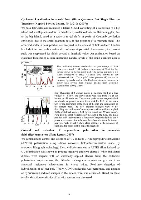
Cyclotron Localization in a sub-10nm Silicon Quantum Dot Single Electron<br />
Transistor (Applied Physics Letters, 90, 032106 (<strong>2007</strong>))<br />
We have fabricated and measured a lateral Si-SET consisting of a succession of a big<br />
island and small quantum dots. In this device, small Coulomb oscillation wiggles, due<br />
to the big island, acted as a scale to reveal shifts in peaks of Coulomb oscillation<br />
envelopes, due to the small quantum dots, in the presence of a magnetic field. The<br />
observed shifts in peak position are analyzed in the context of field-induced Landau<br />
level shift in dots with a soft-wall confinement potential. Furthermore, the current<br />
peak was suppressed for fields beyond a threshold value. An explanation based on<br />
cyclotron localization at non-interacting Landau levels of the small quantum dots is<br />
presented.<br />
The oscillatory current modulation in gate voltage at B=0<br />
(black curve) and B=5T (red curve) measured at 70mK for the<br />
device shown in the top-right inset. The device contains a big<br />
island connected to leads via small dots present in the<br />
nano-constrictions. The top-left inset presents IV b curves at<br />
ramping V g clearly marking the Coulomb blockade diamond; a<br />
closer look reveals fine wiggles arising from Coulomb<br />
oscillation in the big island.<br />
(top) Dynamics of 5 current peaks in magnetic field at a bias<br />
voltage of 1.8 mV. The curves shift with field from -5T at the<br />
bottom to +5T at the top. The current peaks at zero magnetic field<br />
are clearly suppressed as seen from peak P3. Refer to the main<br />
text for the description of the origin of the shift and suppression of<br />
the current peak. The inset presents enlarged view of P5<br />
describing the evolution of current peak position with the applied<br />
fields of 0 (black curve), 2.5T (green curve) and 5T (red curve).<br />
Note also the small wiggles show no shift in the field. The peak<br />
position shift in (bottom) as a function of magnetic field for the 5<br />
peaks are extracted from the raw data shown in (top) for further<br />
analysis. Peaks 2 and 3 show clear splitting in the presence of<br />
field, and the peaks shift in opposite directions.<br />
Control and detection of organosilane polarization on nanowire<br />
field-effect-transistors (Nano Letters, <strong>2007</strong>)<br />
We demonstrated control and detection of UV-induced 3-Aminopropyltriethoxysilane<br />
(APTES) polarization using silicon nanowire field-effect-transistors made by<br />
top-down lithograph technology. Electric dipole moment in APTES films induced by<br />
UV-illumination was shown to produce negative effective charges. When individual<br />
dipoles were aligned with an externally applied electric field, the collective<br />
polarization can prevail over the UV-induced charges in the wires and give rise to an<br />
abnormal resistance enhancement in n-type wires. Real-time detection of<br />
hybridization of 15-mer poly-T/poly-A DNA molecules was performed, and amount<br />
of hybridization induced charges in the silicon wire was estimated. Based on these<br />
results, detection sensitivity of the wire sensors was discussed.<br />
28