Download PDF - Whitesides Research Group - Harvard University
Download PDF - Whitesides Research Group - Harvard University
Download PDF - Whitesides Research Group - Harvard University

Create successful ePaper yourself
Turn your PDF publications into a flip-book with our unique Google optimized e-Paper software.
Fabrication inside Microchannels Using Fluid Flow<br />
Kenis et al.<br />
as macroporous membranes, 16 tunable optical filters, 17 and<br />
3D photonic band gap materials. 18<br />
These studies established the concept of using the<br />
capillary as a small reactor, and identified some of the<br />
types of chemistry that can be carried out using this type<br />
of reactor. The range of structures that one can fabricate<br />
inside microchannels using only a single stream of liquid<br />
is, however, limited.<br />
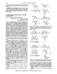
FIGURE 3. Fabrication of near-field optical probes by tube etching<br />
as proposed by Stöckle et al. Schematic of the convection mechanism:<br />
(A) initial diffusion-controlled etchingsmore etchant available<br />
to the outer regions of the fibersand (B) convection-controlled tip<br />
formation inside the tube driven by concentration gradients and the<br />
gravitational removal of reaction products. (C) Optical micrograph<br />
of an uncoated tip. (D) Scanning electron micrographs of an Alcoated<br />
tube-etched fiber tip. Top: the glass surface close to the tip<br />
apex. Bottom: the tip apex. Reproduced with permission from ref<br />
12.<br />
technique. 13 The channel consisted of a poly(dimethylsiloxane)<br />
(PDMS) membrane with a channel structure<br />
embossed in its surface placed on a gold-covered substrate.<br />
The channel was filled with an electroless deposition<br />
solution containing copper ions and formaldehyde<br />
as the reducing agent. The activity of the gold surface in<br />
catalyzing the electroless deposition process resulted in<br />
selective deposition of copper on the wall of the channel<br />
formed by the gold surface and not on the walls of the<br />
channel formed by the PDMS mold.<br />
Similarly, Biebuyck et al. patterned regions of a substrate<br />
with immunoglobulins from a single liquid flow in<br />
a microfluidic network embossed in PDMS that was<br />
placed on the substrate. 14 This PDMS mold was passivated<br />
with poly(ethylene glycol) or bovine serum albumin prior<br />
to placement on the substrate to avoid deposition of<br />
immunoglobulins on its surface.<br />
Arrays of Beads. A related technique also gives access<br />
to crystalline arrays of 0.1-3-µm beads inside 10-100-<br />
µm channels. The liquid flow (driven by evaporation from<br />
one end of the capillary, or by capillary filling of the tube)<br />
delivered the beads from suspension to a region in which<br />
they are, in essence, filtered from the flowing stream; this<br />
flow led to crystalline arrays. Harrison et al. and Manz et<br />
al. have used such arrays as packed reactor beds in<br />
microanalytical devices. 15 Xia et al. have exploited related<br />
flow behavior between narrowly spaced plates to fabricate<br />
crystalline arrays of beads; these crystals may be useful<br />
IV. Microfabrication Using Multiple Streams of<br />
Liquid in Laminar Flow<br />
Soft lithography allows the fabrication of branching capillary<br />
networks rapidly, so long as the capillaries are >20<br />
µm in lateral dimension. 19 The procedure we useswhich<br />
we call “rapid prototyping”sconsists of four steps: (i)<br />
high-resolution printing of a mask with >20-µm features;<br />
(ii) photolithography with this mask to fabricate a basrelief<br />
master; (iii) micromolding against this master to<br />
form three sides of the channel system; and (iv) sealing<br />
to form the complete microchannel. It is straightforward<br />
to create multiple streams of fluids flowing laminarly in<br />
parallel inside these channels 20 and to use these streams<br />
for microfabrication and micropatterning by localized<br />
delivery of reagents from the laminar flows. This methods<br />
sometimes in combination with the use of prepatterned<br />
channelssallows fabrication of complex functional structures<br />
inside preformed capillaries without the registration<br />
steps required by planar photolithography.<br />
Microfabrication by delivery of reactants from parallel<br />
laminar flows generates structures (etched or deposited)<br />
having edges tapered along their longitudinal direction<br />
as a result of diffusion transverse to the direction of<br />
flow. 20,26 This diffusional broadening can be minimized<br />
by using high flow rates (v ≈ 0.50 m s -1 ); high rates of<br />
flow result in short residence times in the region being<br />
patterned. The resolution one can achieve depends on the<br />
details of the process being used for patterning.<br />
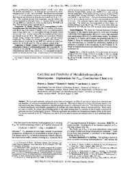
Area-Selective Crystal Growth. A two-stream laminar<br />
flow can be used for the localized nucleation and growth<br />
of crystals inside a microchannel. 20 The capillary is<br />
fabricated by placing a patterned PDMS membrane on a<br />
gold-coated wafer covered with a self-assembled monolayer<br />
(SAM) of HS(CH 2 ) 15 COOH; this SAM nucleates<br />
formation of calcite crystals. 21 Figure 4A shows a line of<br />
calcite crystalsswith diameters of 2-5 µmsthat have<br />
nucleated and grown at the interface between two parallel<br />
streams, one containing calcium ions (as CaCl 2 ) and the<br />
other containing carbonate ions (as NaHCO 3 ).<br />
Patterned Etching of Silver and PDMS. Figure 4B<br />
shows the result of patterning the inside of a glass capillary<br />
by electroless deposition of silver from one stream of a<br />
two-stream fluid flow system. The glass capillary is connected<br />
to a Y-shaped channel in PDMS in order to create<br />
the two-stream flow system; the method can be extended<br />
to four or more streams. 22 Figure 4C shows the creation<br />
of topographical features inside of a PDMS capillary using<br />
patterned flow of etchant and inert solvent. 23 In general,<br />
the position (or edges) of the etched or deposited micro-<br />
844 ACCOUNTS OF CHEMICAL RESEARCH / VOL. 33, NO. 12, 2000