Synthesis, Characterization, and Performance of CdInTe ...
Synthesis, Characterization, and Performance of CdInTe ...
Synthesis, Characterization, and Performance of CdInTe ...

Create successful ePaper yourself
Turn your PDF publications into a flip-book with our unique Google optimized e-Paper software.
40 A.Y. Shenouda et al. / Journal <strong>of</strong> Alloys <strong>and</strong> Compounds 563 (2013) 39–43<br />
solution. Therefore, the hydroxide phase was precipitated. A suitable amount <strong>of</strong><br />
NaBH 4 solution was added to the mixture to reduce the hydroxide phase to the<br />
metalloid alloy. After that, the mixture was stirred with heating at around 85 °C<br />
for 2 h. The solution mixture was left overnight to cool <strong>and</strong> precipitate the metalloid<br />
alloy compound by decantation. Then, the precipitant was filtered out <strong>and</strong> washed<br />
by 1% <strong>of</strong> NaBH 4 solution followed by distilled water. Finally, the prepared powders<br />
were annealed at 300 °C for 2 h in argon atmosphere.<br />
2.2. Physical characterization<br />
The crystalline phases were identified by X-ray diffraction (XRD) on a Brucker<br />
axis D8 diffractometer with crystallographic data s<strong>of</strong>tware Topas 2 using Cu Ka<br />
(k = 1.5406 nm) radiation operating at 40 kV <strong>and</strong> 30 mA. The angle scan rate was<br />
set at 2 °/min. The particles morphology was studied with a scanning electron<br />
microscope (JEOL, model JSM-5040). Elemental compositions <strong>of</strong> the various<br />
Cd 1 x In x Te samples were analyzed by inductively coupled plasma (ICP, Perkin–<br />
Elmer Optima 2000 DV). The UV–vis transmission spectrum was measured by a<br />
UV–vis–NIR spectrophotometer (Jasco-V-570 spectrophotometer, Japan).<br />
2.3. Electrochemical measurements<br />
The electrochemical impedance spectra (EIS) measurements were carried out<br />
using cell holder <strong>of</strong> two electrodes. The samples powders were pressed into pellets<br />
<strong>of</strong> 12 mm diameter <strong>and</strong> 3 mm thickness. The amplitude was 20 mV <strong>and</strong> the frequencies<br />
varied from 10 5 Hz to 10 mHz. For photo electrochemical cell, the working<br />
electrode prepared from Cd 1 x In x Te sample materials was painted on conducting<br />
borosilicate glass substrate (dimensions: 2.5 cm 1.1 cm 7 cm) coated with a<br />
thin film <strong>of</strong> indium tin oxide (ITO). The conducting glass was purchased from SPI<br />
Company, USA.<br />
The active area was 2.5 cm 2.5 cm. Counter electrode was Pt. The cell configuration<br />
was fabricated: Glass/ITO/Cd 1 x In x Te/0.5 M Na 2 S + 0.5 M S + 0.5 M NaOH/Pt<br />
<strong>and</strong> characterized through current–voltage (I–V) measurements using silver halogen<br />
filament light source <strong>of</strong> 500 W [25]. The open circuit potential (V oc ) <strong>and</strong> the<br />
short circuit currents (I sc ) were recorded for the coated active material.<br />
3. Results <strong>and</strong> discussion<br />
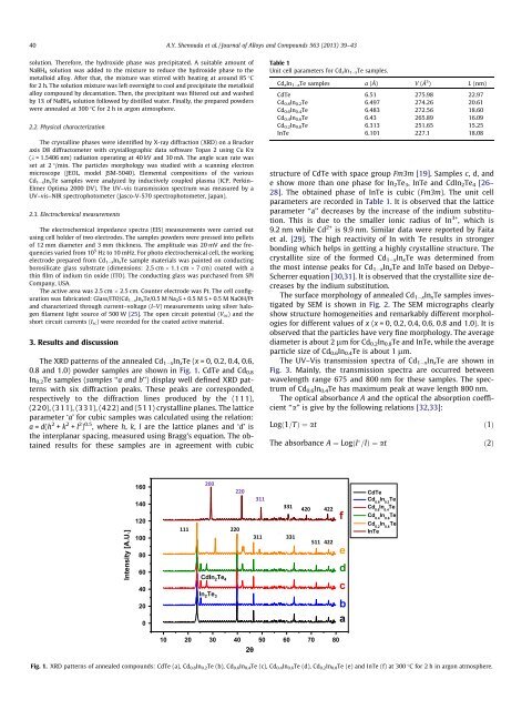
The XRD patterns <strong>of</strong> the annealed Cd 1 x In x Te (x = 0, 0.2, 0.4, 0.6,<br />
0.8 <strong>and</strong> 1.0) powder samples are shown in Fig. 1. CdTe <strong>and</strong> Cd 0.8<br />
In 0.2 Te samples (samples ‘‘a <strong>and</strong> b’’) display well defined XRD patterns<br />
with six diffraction peaks. These peaks are corresponded,<br />
respectively to the diffraction lines produced by the (111),<br />
(220), (311), (331), (422) <strong>and</strong> (511) crystalline planes. The lattice<br />
parameter ‘a’ for cubic samples was calculated using the relation:<br />
a = d(h 2 + k 2 + l 2 ) 0.5 , where h, k, l are the lattice planes <strong>and</strong> ‘d’ is<br />
the interplanar spacing, measured using Bragg’s equation. The obtained<br />
results for these samples are in agreement with cubic<br />
Table 1<br />
Unit cell parameters for Cd x In 1 x Te samples.<br />
Cd x In 1 x Te samples a (Å) V (Å 3 ) L (nm)<br />
CdTe 6.51 275.98 22.97<br />
Cd 0.8 In 0.2 Te 6.497 274.26 20.61<br />
Cd 0.6 In 0.4 Te 6.483 272.56 18.60<br />
Cd 0.4 In 0.6 Te 6.43 265.89 16.09<br />
Cd 0.2 In 0.8 Te 6.313 251.65 15.25<br />
InTe 6.101 227.1 18.08<br />
structure <strong>of</strong> CdTe with space group Fm3m [19]. Samples c, d, <strong>and</strong><br />
e show more than one phase for In 2 Te 3 , InTe <strong>and</strong> CdIn 2 Te 4 [26–<br />
28]. The obtained phase <strong>of</strong> InTe is cubic (Fm3m). The unit cell<br />
parameters are recorded in Table 1. It is observed that the lattice<br />
parameter ‘‘a’’ decreases by the increase <strong>of</strong> the indium substitution.<br />
This is due to the smaller ionic radius <strong>of</strong> In 3+ , which is<br />
9.2 nm while Cd 2+ is 9.9 nm. Similar data were reported by Faita<br />
et al. [29]. The high reactivity <strong>of</strong> In with Te results in stronger<br />
bonding which helps in getting a highly crystalline structure. The<br />
crystallite size <strong>of</strong> the formed Cd 1 x In x Te was determined from<br />
the most intense peaks for Cd 1 x In x Te <strong>and</strong> InTe based on Debye–<br />
Scherrer equation [30,31]. It is observed that the crystallite size decreases<br />
by the indium substitution.<br />
The surface morphology <strong>of</strong> annealed Cd 1 x In x Te samples investigated<br />
by SEM is shown in Fig. 2. The SEM micrographs clearly<br />
show structure homogeneities <strong>and</strong> remarkably different morphologies<br />
for different values <strong>of</strong> x (x = 0, 0.2, 0.4, 0.6, 0.8 <strong>and</strong> 1.0). It is<br />
observed that the particles have very fine morphology. The average<br />
diameter is about 2 lm for Cd 0.2 In 0.8 Te <strong>and</strong> InTe, while the average<br />
particle size <strong>of</strong> Cd 0.6 In 0.4 Te is about 1 lm.<br />
The UV–Vis transmission spectra <strong>of</strong> Cd 1 x In x Te are shown in<br />
Fig. 3. Mainly, the transmission spectra are occurred between<br />
wavelength range 675 <strong>and</strong> 800 nm for these samples. The spectrum<br />
<strong>of</strong> Cd 0.6 In 0.4 Te has maximum peak at wave length 800 nm.<br />
The optical absorbance A <strong>and</strong> the optical the absorption coefficient<br />
‘‘a’’ is give by the following relations [32,33]:<br />
Logð1=TÞ ¼at<br />
The absorbance A ¼ LogðI =IÞ ¼at<br />
ð1Þ<br />
ð2Þ<br />
Intensity [A.U.]<br />
160<br />
140<br />
120<br />
100<br />
80<br />
60<br />
40<br />
20<br />
0<br />
CdIn 2 Te 4<br />
In 2 Te 3<br />
f<br />
e<br />
d<br />
c<br />
b<br />
a<br />
CdTe<br />
Cd 0.8<br />
In 0.2<br />
Te<br />
Cd 0.6<br />
In 0.4<br />
Te<br />
Cd 0.4<br />
In 0.6<br />
Te<br />
Cd 0.2<br />
In 0.8<br />
Te<br />
InTe<br />
10 20 30 40 50 60 70 80<br />
2θθ<br />
Fig. 1. XRD patterns <strong>of</strong> annealed compounds: CdTe (a), Cd 0.8 In 0.2 Te (b), Cd 0.6 In 0.4 Te (c), Cd 0.4 In 0.6 Te (d), Cd 0.2 In 0.8 Te (e) <strong>and</strong> InTe (f) at 300 °C for 2 h in argon atmosphere.