Semiconductor Industry Brochure - Siemens PLM Software
Semiconductor Industry Brochure - Siemens PLM Software
Semiconductor Industry Brochure - Siemens PLM Software

Create successful ePaper yourself
Turn your PDF publications into a flip-book with our unique Google optimized e-Paper software.
www.siemens.com/plm/hightech<br />
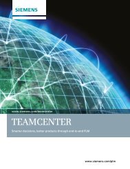
Optimizing semiconductor device<br />
innovation practices and processes<br />
Smarter decisions, better products<br />
www.siemens.com/plm
“If you examine what SOC-design<br />
teams are doing, you’ll find that<br />
creating an SOC is a process of<br />
finding, characterizing, and<br />
assembling previously used IP.”<br />
Electronics Design News, August 11, 2011<br />
2<br />
2
Next-generation solution to get more<br />
out of semiconductor R&D<br />
“Today, there are nearly a billion<br />
transistors per human, and each<br />
one costs one ten-millionth of a<br />
cent. Yes, some of these transistors<br />
are going into servers, PCs, smart<br />
phones, MP3 players and tablets.<br />
But an increasing number of them<br />
are going into appliances and automobiles,<br />
power grids, roadways,<br />
railways and waterways.”<br />
IBM CEO Samuel J. Palmisano, 2011<br />
<strong>Siemens</strong> <strong>PLM</strong> <strong>Software</strong> is a proven leader in providing<br />
solutions for managing semiconductor devices from<br />
concept ideation through end-of-life. Our solutions enable<br />
you to optimize your return on R&D investments, re-use<br />
your valuable intellectual property (IP) and know-how and<br />
leverage the massive innovation power of your value chain<br />
partners. These capabilities enable you to bring the right<br />
systems-on-chip (SoC), integrated circuits (IC) and other<br />
products to market with greater confidence, greater ROI,<br />
faster time-to-market, improved quality and better<br />
collaboration among partners.<br />
<strong>Siemens</strong> <strong>PLM</strong> <strong>Software</strong>’s solutions for the semiconductor<br />
device industry enable you to effectively manage semiconductor<br />
design and manufacturing complexities with a complete<br />
set of unified applications that accelerate new device<br />
introduction, improve productivity, lower production costs<br />
and facilitate design for sustainability and environmental<br />
compliance.<br />
<strong>Siemens</strong> <strong>PLM</strong> <strong>Software</strong> provides unique capabilities that<br />
enable semiconductor companies to:<br />
• Optimize their semiconductor device R&D innovation<br />
pipeline throughout the device lifecycle<br />
• Unify the decision making processes for the complex<br />
design of SoC, IC and IP<br />
• Maximize the safe re-use of proven IP in device design<br />
and fabrication<br />
• Build a secure and scalable collaboration platform within<br />
the enterprise and with semiconductor value chain<br />
partners<br />
• Facilitate the device design for sustainability objectives<br />
• Increase the participation of all decision stakeholders in<br />
the device design management processes with mobility<br />
and context-aware applications<br />
3
Challenges in the<br />
semiconductor device<br />
industry<br />
”Many institutions have a<br />
history of time and budget<br />
overruns, in addition to late<br />
adjustments to product<br />
specifications from the R&D<br />
department, resulting in<br />
angry customers. At the same<br />
time, changing customer<br />
expectations and requests for<br />
specifications lead to many<br />
new projects in the pipeline.”<br />
McKinsey & Company, “Getting Mo(o)re<br />
out of semiconductor R&D”<br />
Today’s semiconductor device makers are<br />
feeling the increasing impact of disruptive<br />
forces from multiple fronts. Hyperfragmented<br />
market needs, escalating<br />
design costs, growing product complexity,<br />
shrinking average sales prices and the<br />
relentless pace of innovation are creating<br />
intense pressures on the industry.<br />
Coupled with the industry’s daunting<br />
design challenges, accelerated lifecycles<br />
and complex supply chains, it is no<br />
wonder that product launch dates, development<br />
budgets and quality targets are<br />
frequently missed.<br />
Device makers are being challenged by<br />
rapidly-evolving business models based<br />
on the collaboration between fabless (or<br />
fab-lite) and foundry companies, the<br />
increasing demands for complete turnkey<br />
solutions for niche markets, the difficulty<br />
to fulfill commitments to customers<br />
on schedule and at cost and the escalating<br />
complexities in both device design<br />
and operational processes that are distributed<br />
globally.<br />
Not content with the past success formulas,<br />
device makers are embracing a new<br />
set of design best practices centered on<br />
collaborative SoC and IC design management.<br />
These practices promise to align<br />
their R&D investments closer to market<br />
needs, bring in IP partners and foundries<br />
into the design process in a secure environment<br />
and manage the inherent complexities<br />
to gain a competitive advantage.<br />
<strong>Siemens</strong> <strong>PLM</strong> <strong>Software</strong> has worked with<br />
the leaders in the semiconductor ecosystem<br />
to understand the industry’s needs<br />
and provide collaborative device design<br />
management solutions to meet these<br />
challenges.<br />
4
“The ratio of product lifecycle<br />
to product development time<br />
in semiconductors is half<br />
that for a mobile phone and<br />
a third that for an automobile.<br />
And for the growing<br />
ranks of “fab lite” or fabless<br />
players, R&D excellence is the<br />
key differentiating factor.<br />
McKinsey & Company, “Getting Mo(o)re out of<br />
semiconductor R&D”<br />
5
Vision<br />
<strong>Siemens</strong> <strong>PLM</strong> <strong>Software</strong> has a clear vision that guides the<br />
development and investment in solutions consistent with<br />
the needs and aspirations of the leading device makers.<br />
This vision promises to bring about best practices to help<br />
device makers manage the process of developing SoC and<br />
IC devices. The vision centers on smarter decision making<br />
for the development of devices.<br />
To create the best possible platform for collaborative<br />
decision support for device makers, we are investing in<br />
three main areas to fulfill that vision:<br />
An Intelligently Integrated Information environment<br />
that links all of the design information and program<br />
management data in an unified fashion, across the key<br />
domains. This includes new device introduction stakeholder<br />
organizations that may be outside the four walls of<br />
the device makers. We not only understand how device<br />
design and program information are related, but why that<br />
relationship exists. This gives management, design teams<br />
and partners unique abilities to start predicting what IP<br />
and other design information they’ll need and when they’ll<br />
need it, so the system can start proactively delivering the<br />
right information instead of making the users go find it.<br />
Building that environment on a next-generation<br />
future-proof architecture that ensures our customer’s<br />
IT investment will continue to evolve in concert<br />
with ours.<br />
We will also ensure that you have a high-definition user<br />
experience that proactively delivers the right information<br />
to you. This is how mobility and context-aware applications<br />
fit in our vision.<br />
7
Smarter decisions, better<br />
products for semiconductor<br />
devices through innovation<br />
management across the<br />
value chain<br />
“Moore’s law describes a<br />
long-term trend in the history<br />
of computing hardware: the<br />
number of transistors that can<br />
be placed inexpensively on an<br />
integrated circuit doubles<br />
approximately every two<br />
years.”<br />
Wikipedia<br />
<strong>Siemens</strong> <strong>PLM</strong> <strong>Software</strong> provides a unified<br />
solution platform to ensure a single<br />
authoritative source of product and process<br />
information throughout the semiconductor<br />
device design lifecycle in a<br />
globally distributed value chain.<br />
<strong>Semiconductor</strong> device makers are always<br />
on the leading edge of product innovation<br />
and the application of the latest<br />
technological breakthroughs, but they<br />
have increasingly realized that they need<br />
to invest more in development lifecycle<br />
management processes and disciplines in<br />
order to get more out of their R&D<br />
investments.<br />
The industry’s innovative and early adopters<br />
of this comprehensive device development<br />
management solution benefited<br />
from acquiring enhanced or new capabilities<br />
including SoC/IC R&D pipeline optimization,<br />
SoC and IC design information and<br />
program management, IP re-use and legal<br />
protection, device software process management,<br />
design for sustainability and<br />
compliance and greater organizational<br />
productivity through innovative application<br />
of mobility and context aware social<br />
development.<br />
8
<strong>Siemens</strong> <strong>PLM</strong> <strong>Software</strong> has worked with<br />
industry leaders in the United States,<br />
Europe and Asia Pacific regions. These<br />
pioneers include integrated design<br />
manufacturers (IDM), fabless device<br />
makers and foundries.<br />
<strong>Siemens</strong> <strong>PLM</strong> <strong>Software</strong> has closely<br />
collaborated and co-innovated with<br />
these industry leaders across the entire<br />
semiconductor value chain to define and<br />
capture the best practices and model<br />
the most promising management<br />
processes in a single unified enterprise<br />
solution architecture.<br />
9
“Getting quality chip designs<br />
out the door takes super-human<br />
effort.”<br />
Kalypso Research, “<strong>Semiconductor</strong> Product<br />
Lifecycle Management”<br />
Optimizing the IC/IP innovation pipeline<br />
Our IC/IP investment pipeline optimization solution focuses<br />
on the strategic aspect of device development processes,<br />
enabling customer needs, requirements management,<br />
portfolio management and program management.<br />
Customer needs and requirements management enable<br />
you to link, define, allocate, track and communicate market<br />
requirements with full traceability to architecture, design<br />
and fabrication artifacts. This end-to-end traceability<br />
ensures solution integrity and is a critical management<br />
lever for quality and customer satisfaction.<br />
Portfolio management enables you to increase your ROI<br />
by focusing your critical financial and human resources on<br />
the most promising ideas.<br />
Program management enables you to drive planning<br />
based on requirements and to manage execution of work<br />
tasks and deliverables all in one system.<br />
Unified SoC/IC design management<br />
SoC/IC design management enables you to establish a<br />
single authoritative system to define, create, change and<br />
configure SoC/IC program requirements, schedules, phase<br />
gate or task deliverables, risks, changes, tape-out design<br />
release and archival, gate review checklists, issues and<br />
errata, IC maturity status, test programs and validation<br />
results.<br />
Global Enterprise IP Catalog Management<br />
You can design and engineer solutions much faster at lower<br />
costs by re-using your own and your partners’ IP, as well as<br />
by licensing your IP to other companies in the value chain to<br />
create new sources of revenue and expand the entire semiconductor<br />
ecosystem. <strong>Siemens</strong> <strong>PLM</strong> <strong>Software</strong>’s unique IP<br />
catalog management capabilities deliver global scalability,<br />
easy classification, navigation, search, legal team review,<br />
quality management and safe re-use, without legal and<br />
quality concerns.<br />
10
“Like many other top innovators, Silicon<br />
Valley companies not only have found<br />
success in creating path-breaking new<br />
technologies, but are almost twice as<br />
likely as average companies to have<br />
developed capabilities that provide a<br />
superior understanding of the stated<br />
and unstated needs of their end customers.<br />
It isn’t just about how many<br />
transistors you can fit on a chip, but<br />
also about how such advances can<br />
lead to products and services that gain<br />
unprecedented traction in the marketplace<br />
through superior insight into<br />
customers, as well as the development<br />
of practical value propositions that<br />
will win those customers’ business.”<br />
Booz & Company, “The Global Innovation 1000:<br />
Why Culture Is Key”<br />
Secure collaboration across your value chain<br />
Our solutions enable your product teams to work with<br />
your suppliers, IP partners, foundries and customers<br />
in a secure and collaborative environment that facilitates<br />
design issues and change management as well as IP/IC<br />
design data exchange by program or platform specific<br />
reviews. <strong>Siemens</strong> <strong>PLM</strong> <strong>Software</strong> takes pride in working with<br />
the world’s most innovative and largest semiconductor<br />
companies that demand secure, scalable and flexible<br />
collaboration infrastructure and methodologies.<br />
Design for sustainability<br />
<strong>Industry</strong> leaders are no longer limiting their efforts to<br />
prove device compliances, as important as that is. They<br />
are also adopting a design for sustainability mentality<br />
across the product lifecycle to seek market and<br />
technological advantages. <strong>Siemens</strong> <strong>PLM</strong> <strong>Software</strong><br />
delivers a full lifecycle solution to build up a model<br />
of the “cradle-to-grave” impacts for a new device, to<br />
manage the sustainability and environmental compliance<br />
requirements including carbon footprint, energy usage<br />
and various jurisdictions’ RoHS regulations, WEEE, EOL,<br />
EuP and REACH.<br />
Mobile and context-aware social development<br />
The next-generation solution for semiconductor device<br />
lifecycle management features critical capabilities, such<br />
as mobility and context-awareness, to boost productivity<br />
and embrace social aspects of device development<br />
programs across the value chain. Teamcenter® Mobility<br />
software extends your device development environment by<br />
providing always-on access, improving productivity by<br />
enabling the decisions to be made anywhere, anytime with<br />
mobile <strong>PLM</strong>. Context-aware interactions with your <strong>PLM</strong> environment<br />
focus your knowledge workers on the decisions<br />
and tasks. Relevant contexts are brought to the users<br />
through intelligent navigation, aggregation and application<br />
of relevant device program management and design data<br />
dynamically, thus shortening the learning curve and<br />
improving decision quality and productivity.<br />
11
Next-generation solution<br />
adoption and benefits<br />
<strong>Siemens</strong> <strong>PLM</strong> <strong>Software</strong> has worked with<br />
the industry leaders of integrated semiconductor<br />
design companies, fabless<br />
wireless SoC companies, top foundries<br />
and equipment makers. Our customers<br />
have embraced <strong>PLM</strong> as the platform to<br />
make smarter decisions on resources,<br />
capacities, customer needs, SoC/IC design<br />
changes, issues and bugs, and IP re-use.<br />
They have the peace of mind knowing<br />
that <strong>Siemens</strong> <strong>PLM</strong> <strong>Software</strong>’s solutions<br />
ensure the secrecy and security of their IP<br />
when shared in an extended value chain.<br />
Our customers have been able to achieve<br />
real business value in time-to-market<br />
improvements by improving key operational<br />
areas such as:<br />
• Significantly reduce the tape-out<br />
defects and mask set costs<br />
• Improve design re-use across device<br />
programs<br />
• Greater productivity through effective<br />
talent/capacity management<br />
• Greater device quality through end-toend<br />
traceability and impact analysis<br />
• Trusted collaboration among device<br />
makers, IP providers and foundries<br />
12
According to management consultancy<br />
firm Kalypso’s study of 25 top semiconductor<br />
companies, best-in-class companies<br />
employing a strategic <strong>PLM</strong> program<br />
reported seeing increased business benefits<br />
in the following areas:<br />
Our findings are consistent with Kalypso’s<br />
conclusions that leaders embrace <strong>PLM</strong> as<br />
not only technology transformations but<br />
also as a strategic enabler of their corporate<br />
innovation objectives.<br />
• 100 percent improved hitting their<br />
launch dates<br />
• 84 percent experienced an increase in<br />
hitting revenue targets<br />
• 89 percent achieved better product<br />
cost targets<br />
• 95 percent improved their ability<br />
to meet development budgets<br />
• 98 percent increased their ability to<br />
hit quality targets<br />
13
<strong>Siemens</strong> <strong>PLM</strong> <strong>Software</strong><br />
leadership and<br />
next-generation platform<br />
advantages<br />
“IC companies are not just<br />
building discrete semiconductor<br />
components. Many of them<br />
are building entire systems on<br />
a chip. Among the consequences<br />
are the facts that pressures on<br />
manufacturing cycle times<br />
have increased significantly<br />
and the level of work required<br />
up and down the value chain<br />
has increased with it.”<br />
Rick Cassidy, President, TSMC<br />
North America<br />
<strong>Siemens</strong> <strong>PLM</strong> <strong>Software</strong> is a leading <strong>PLM</strong><br />
supplier to the entire semiconductor<br />
ecosystem including device makers,<br />
equipment makers and foundries. We are<br />
customer-focused and have collaborated<br />
with semiconductor industry leaders to<br />
develop industry specific best practice<br />
based solutions.<br />
Our customers include the largest and<br />
most innovative semiconductor device<br />
companies in the world. For example,<br />
<strong>Siemens</strong> <strong>PLM</strong> <strong>Software</strong> solutions have<br />
been helping the world’s largest integrated<br />
device manufacturer with a<br />
series of transformational <strong>PLM</strong> initiatives<br />
aimed at improving time-to-market and<br />
productivity. We also work with one of<br />
the fastest growing fabless companies to<br />
optimize SoC, IC and IP development<br />
processes. We have also been collaborating<br />
with a top foundry to enable its<br />
strategic initiatives in providing a scalable<br />
and secure open innovation platform.<br />
<strong>Siemens</strong> <strong>PLM</strong> <strong>Software</strong> is a next-generation,<br />
unified platform that accelerates<br />
and dramatically improves product and<br />
process innovation for semiconductor<br />
device makers including integrated device<br />
manufacturers, fablite or fabless device<br />
makers and foundries. Our solution is<br />
built on a unified architecture, single<br />
data model, with industry best practice<br />
workflows connecting semiconductor<br />
device makers’ customers, IP providers,<br />
foundries and the core business<br />
functions within. These capabilities<br />
meet the core needs of device makers,<br />
including R&D pipeline and asset<br />
optimization, unified SoC/IC design<br />
management, global enterprise IP catalog<br />
management, secure collaboration across<br />
the value chain players, design for<br />
sustainability and compliance objectives,<br />
mobility and context-aware social<br />
development.<br />
14
<strong>Siemens</strong> <strong>Industry</strong> <strong>Software</strong><br />
Headquarters<br />
Granite Park One<br />
5800 Granite Parkway<br />
Suite 600<br />
Plano, TX 75024<br />
USA<br />
+1 972 987 3000<br />
Fax +1 972 987 3398<br />
Americas<br />
Granite Park One<br />
5800 Granite Parkway<br />
Suite 600<br />
Plano, TX 75024<br />
USA<br />
+1 800 498 5351<br />
Fax +1 972 987 3398<br />
Europe<br />
3 Knoll Road<br />
Camberley<br />
Surrey GU15 3SY<br />
United Kingdom<br />
+44 (0) 1276 702000<br />
Fax +44 (0) 1276 702130<br />
Asia-Pacific<br />
Suites 6804-8, 68/F<br />
Central Plaza<br />
18 Harbour Road<br />
WanChai<br />
Hong Kong<br />
+852 2230 3333<br />
Fax +852 2230 3210<br />
About <strong>Siemens</strong> <strong>PLM</strong> <strong>Software</strong><br />
<strong>Siemens</strong> <strong>PLM</strong> <strong>Software</strong>, a business unit of the <strong>Siemens</strong><br />
<strong>Industry</strong> Automation Division, is a leading global provider<br />
of product lifecycle management (<strong>PLM</strong>) software and<br />
services with nearly 6.7 million licensed seats and 69,500<br />
customers worldwide. Headquartered in Plano, Texas,<br />
<strong>Siemens</strong> <strong>PLM</strong> <strong>Software</strong> works collaboratively with<br />
companies to deliver open solutions that help them<br />
turn more ideas into successful products. For more<br />
information on <strong>Siemens</strong> <strong>PLM</strong> <strong>Software</strong> products and<br />
services, visit www.siemens.com/plm.<br />
© 2012 <strong>Siemens</strong> Product Lifecycle<br />
Management <strong>Software</strong> Inc. All rights<br />
reserved. <strong>Siemens</strong> and the <strong>Siemens</strong><br />
logo are registered trademarks of<br />
<strong>Siemens</strong> AG. D-Cubed, Femap,<br />
Geolus, GO <strong>PLM</strong>, I-deas, Insight,<br />
JT, NX, Parasolid, Solid Edge,<br />
Teamcenter, Tecnomatix and Velocity<br />
Series are trademarks or registered<br />
trademarks of <strong>Siemens</strong> Product Lifecycle<br />
Management <strong>Software</strong> Inc. or<br />
its subsidiaries in the United States<br />
and in other countries. All other<br />
logos, trademarks, registered trademarks<br />
or service marks used herein<br />
are the property of their respective<br />
holders.<br />
22413-X21 1/12 A