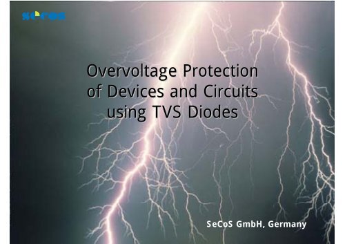
Overvoltage Protection of Devices and Circuits using TVS ... - SeCoS
Overvoltage Protection of Devices and Circuits using TVS ... - SeCoS
Overvoltage Protection of Devices and Circuits using TVS ... - SeCoS
- No tags were found...

Create successful ePaper yourself
Turn your PDF publications into a flip-book with our unique Google optimized e-Paper software.
<strong>Overvoltage</strong> <strong>Protection</strong><br />
<strong>of</strong> <strong>Devices</strong> <strong>and</strong> <strong>Circuits</strong><br />
<strong>using</strong> <strong>TVS</strong> Diodes<br />
<strong>SeCoS</strong> GmbH, Germany
Inhalt Contents<br />
• <strong>SeCoS</strong> in Kürze <strong>SeCoS</strong> in brief<br />
• Was ist eine <strong>TVS</strong> Diode What is a <strong>TVS</strong> diode<br />
• <strong>TVS</strong> oder Zener <strong>TVS</strong> versus Zener<br />
• Applikationsbeispiele Application examples<br />
• Auswahl des richtigen Bauelements<br />
How to select the optimum device<br />
1
Was ist eine <strong>TVS</strong> Diode<br />
What is a <strong>TVS</strong> diode<br />
I F<br />
V C V BR V WM<br />
I D<br />
V F<br />
I T<br />
I PP<br />
• Kennlinie wie eine Zenerdiode Curve like Zener diode<br />
• Bidirektionale Version erhältlich! Bidirectional Version available!<br />
2
Was ist eine <strong>TVS</strong> Diode<br />
What is a <strong>TVS</strong> diode<br />
Transient<br />
voltage +<br />
clamped<br />
voltage +<br />
peak<br />
current<br />
circuit to<br />
protect<br />
Transient<br />
voltage -<br />
clamped<br />
voltage -<br />
Überspannungsschutz! <strong>Overvoltage</strong> <strong>Protection</strong>!<br />
⇒ Transient Voltage Suppressor<br />
3
<strong>TVS</strong> oder Zenerdiode<br />
<strong>TVS</strong> versus Zener diode<br />
<strong>TVS</strong><br />
– Unterdrückung von<br />
Spannungsspitzen<br />
Suppression <strong>of</strong> transient<br />
voltages<br />
Zener<br />
– Stabilisierung einer<br />
Gleichspannung<br />
Stabilization <strong>of</strong> a DC<br />
voltage<br />
– Auswahlparameter<br />
Parameters for selection:<br />
• V WM Sperrspannung<br />
St<strong>and</strong>-<strong>of</strong>f voltage<br />
• V C Begrenzerspannung<br />
Clamping voltage<br />
• P PPM Impulsverlustleistung<br />
Peak pulse power<br />
– Auswahlparameter<br />
Parameters for selection:<br />
• V Z Zenerspannung<br />
Zener voltage<br />
• P tot Statische Verlustleistung<br />
Steady state power dissip.<br />
4
Gate-Ansteuerung<br />
Gate Control<br />
• Gate-Schutz:<br />
1 bidirektionale <strong>TVS</strong>- ersetzt<br />
2 antiserielle Zener-Dioden<br />
on request:<br />
2 in 1!<br />
2 in 1!<br />
Gate <strong>Protection</strong>:<br />
1 bidirectional <strong>TVS</strong> replaces<br />
2 anti serial Zener diodes<br />
• Aktive Spannungsbegrenzung:<br />
Zener-Dioden st<strong>and</strong>ardmäßig bis<br />
200 V, <strong>TVS</strong> bis 440 V!<br />
Active Clamping:<br />
St<strong>and</strong>ard Zener diodes up to 200 V,<br />
<strong>TVS</strong> up to 440 V!<br />
5
„Crow Bar“ Schaltung<br />
Crow bar circuit<br />
Mit/with Diac:<br />
Mit/with <strong>TVS</strong>:<br />
6
<strong>TVS</strong> Dioden in Schaltnetzteilen<br />
<strong>TVS</strong> diodes in SMPS<br />
Beispiel: Sperrw<strong>and</strong>ler Example: flyback<br />
converter<br />
5 V=<br />
230 V~<br />
7
Auswahl des optimalen Bauteils<br />
Beispiel:<br />
Klemmkreis eines 10 W-Sperrw<strong>and</strong>lers, Eingangsspannung 230 V~,<br />
Spitzenstrom primärseitig 150 mA, Sperrspannung MOSFET 1000 V<br />
1. Sperrspannung der <strong>TVS</strong>-Diode V WM ≈√2 x 230 V ≈ 330 V, z. B. 324 V<br />
Netztoleranz +10%: √2 x 250 V = 353 V < 360 V = V BRmin √<br />
2. Begrenzerspannung der <strong>TVS</strong>-Diode mit V WM = 324 V: V C = 574 V<br />
⇒ Maximale Spannung am MOSFET: 574 V + 330 V = 904 V √<br />
3. Impulsstrom I PPM ≥ 150 mA ⇒ P4KE400C mit I PPM = 730 mA √<br />
Dauer-Verlustleistung ca. 500 mW ⇒ P4KE400C mit P M(AV) = 1 W √<br />
4. Alternativ: 2 x TGL34-200C (SMD MiniMELF!) in Reihe<br />
8
Selecting the optimum device<br />
Example:<br />
Clamping circuit <strong>of</strong> a 10 W flyback converter, input voltage 230 V AC ,<br />
primary peak current 150 mA, MOSFET blocking voltage 1000 V<br />
1. St<strong>and</strong>-<strong>of</strong>f voltage <strong>of</strong> <strong>TVS</strong> diode V WM ≈√2 x 230 V ≈ 330 V, e. g. 324 V<br />
Mains tolerance +10%: √2 x 250 V = 353 V < 360 V = V BRmin √<br />
2. Clamping voltage <strong>of</strong> <strong>TVS</strong> diode (V WM = 324 V): V C = 574 V<br />
⇒ Maximum appearing MOSFET voltage: 574 V + 330 V = 904 V √<br />
3. Peak pulse current I PPM ≥ 150 mA ⇒ P4KE400C with I PPM = 730 mA √<br />
Steady state power dissipation ~ 500 mW ⇒ P4KE400C with P M(AV) = 1<br />
W √<br />
4. Alternatively: 2 x SMAJ200A (SMD MiniMELF!) in series<br />
9
Danke<br />
Thank you