- Page 2 and 3: In Praise of Computer Organization
- Page 4 and 5: F I F T H E D I T I O N Computer Or
- Page 8 and 9: To Linda, who has been, is, and alw
- Page 16 and 17: Preface The most beautiful thing we
- Page 19 and 20: xviii Preface learning more about f
- Page 21 and 22: xx Preface once again like a tightr
- Page 23 and 24: xxii Preface Li (Arizona State Univ
- Page 25: 1 Civilization advances by extendin
- Page 28: 1.1 Introduction 5 Classes of Compu
- Page 33: 10 Chapter 1 Computer Abstractions
- Page 39 and 40: 16 Chapter 1 Computer Abstractions
- Page 41 and 42: 18 Chapter 1 Computer Abstractions
- Page 43 and 44: 20 Chapter 1 Computer Abstractions
- Page 46 and 47: 1.4 Under the Covers 23 To distingu
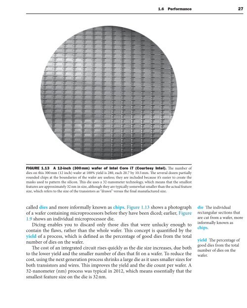
- Page 52 and 53: 1.6 Performance 29 purchasers and t
- Page 54 and 55: 1.6 Performance 31 In discussing a
- Page 56 and 57: 1.6 Performance 33 some application
- Page 58 and 59: 1.6 Performance 35 CPU time for B c
- Page 64 and 65: 1.7 The Power Wall 41 Although powe
- Page 70 and 71: 1.9 Real Stuff: Benchmarking the In
- Page 72 and 73: 1.10 Fallacies and Pitfalls 49 boil
- Page 74: 1.10 Fallacies and Pitfalls 51 is t
- Page 79 and 80: 56 Chapter 1 Computer Abstractions
- Page 81 and 82: 58 Chapter 1 Computer Abstractions
- Page 83: 2 I speak Spanish to God, Italian t
- Page 91 and 92: 68 Chapter 2 Instructions: Language
- Page 93 and 94: 70 Chapter 2 Instructions: Language
- Page 97 and 98: 74 Chapter 2 Instructions: Language
- Page 99 and 100:
76 Chapter 2 Instructions: Language
- Page 101 and 102:
78 Chapter 2 Instructions: Language
- Page 104 and 105:
2.5 Representing Instructions in th
- Page 106 and 107:
2.5 Representing Instructions in th
- Page 111 and 112:
88 Chapter 2 Instructions: Language
- Page 114 and 115:
2.7 Instructions for Making Decisio
- Page 116 and 117:
2.7 Instructions for Making Decisio
- Page 118:
2.7 Instructions for Making Decisio
- Page 121 and 122:
98 Chapter 2 Instructions: Language
- Page 123 and 124:
100 Chapter 2 Instructions: Languag
- Page 125 and 126:
102 Chapter 2 Instructions: Languag
- Page 128:
2.8 Supporting Procedures in Comput
- Page 131 and 132:
108 Chapter 2 Instructions: Languag
- Page 133:
110 Chapter 2 Instructions: Languag
- Page 136 and 137:
2.10 MIPS Addressing for 32-bit Imm
- Page 139:
116 Chapter 2 Instructions: Languag
- Page 143 and 144:
120 Chapter 2 Instructions: Languag
- Page 145:
122 Chapter 2 Instructions: Languag
- Page 148 and 149:
2.12 Translating and Starting a Pro
- Page 150 and 151:
2.12 Translating and Starting a Pro
- Page 152 and 153:
2.12 Translating and Starting a Pro
- Page 156:
2.13 A C Sort Example to Put It All
- Page 159 and 160:
136 Chapter 2 Instructions: Languag
- Page 161:
138 Chapter 2 Instructions: Languag
- Page 166:
2.14 Arrays versus Pointers 143 Poi
- Page 171:
148 Chapter 2 Instructions: Languag
- Page 175 and 176:
152 Chapter 2 Instructions: Languag
- Page 177 and 178:
154 Chapter 2 Instructions: Languag
- Page 179 and 180:
156 Chapter 2 Instructions: Languag
- Page 181:
158 Chapter 2 Instructions: Languag
- Page 185:
162 Chapter 2 Instructions: Languag
- Page 189 and 190:
166 Chapter 2 Instructions: Languag
- Page 191 and 192:
168 Chapter 2 Instructions: Languag
- Page 193 and 194:
170 Chapter 2 Instructions: Languag
- Page 195 and 196:
172 Chapter 2 Instructions: Languag
- Page 197 and 198:
174 Chapter 2 Instructions: Languag
- Page 199:
3 Arithmetic for Computers Numerica
- Page 204:
3.2 Addition and Subtraction 181 mo
- Page 208:
3.3 Multiplication 185 Start Multip
- Page 212:
3.4 Division 189 3.4 Division The r
- Page 216:
3.4 Division 193 Elaboration: The o
- Page 220 and 221:
3.5 Floating Point 197 Computer ari
- Page 222 and 223:
3.5 Floating Point 199 Single preci
- Page 224 and 225:
3.5 Floating Point 201 Floating-Poi
- Page 226 and 227:
3.5 Floating Point 203 Floating-Poi
- Page 229 and 230:
206 Chapter 3 Arithmetic for Comput
- Page 231:
208 Chapter 3 Arithmetic for Comput
- Page 234:
3.5 Floating Point 211 Step 5. Sinc
- Page 237 and 238:
214 Chapter 3 Arithmetic for Comput
- Page 239 and 240:
216 Chapter 3 Arithmetic for Comput
- Page 241 and 242:
218 Chapter 3 Arithmetic for Comput
- Page 245:
222 Chapter 3 Arithmetic for Comput
- Page 250 and 251:
3.8 Going Faster: Subword Paralleli
- Page 252 and 253:
3.9 Fallacies and Pitfalls 229 3.9
- Page 254 and 255:
3.9 Fallacies and Pitfalls 231 Desp
- Page 256:
3.10 Concluding Remarks 233 selecte
- Page 260 and 261:
3.12 Exercises 237 3.12 Exercises 3
- Page 262 and 263:
3.12 Exercises 239 3.23 [10] Write
- Page 264 and 265:
3.12 Exercises 241 3.40 [10] Based
- Page 268 and 269:
4.1 Introduction 245 However, it il
- Page 270:
4.1 Introduction 247 on a load and
- Page 279 and 280:
256 Chapter 4 The Processor PC + 4
- Page 281:
258 Chapter 4 The Processor Instruc
- Page 286:
4.4 A Simple Implementation Scheme
- Page 291:
268 Chapter 4 The Processor 3. The
- Page 294 and 295:
4.4 A Simple Implementation Scheme
- Page 297 and 298:
274 Chapter 4 The Processor pipelin
- Page 300 and 301:
4.5 An Overview of Pipelining 277 P
- Page 302:
4.5 An Overview of Pipelining 279 T
- Page 310 and 311:
4.6 Pipelined Datapath and Control
- Page 312 and 313:
4.6 Pipelined Datapath and Control
- Page 314 and 315:
4.6 Pipelined Datapath and Control
- Page 316 and 317:
4.6 Pipelined Datapath and Control
- Page 318 and 319:
4.6 Pipelined Datapath and Control
- Page 320:
4.6 Pipelined Datapath and Control
- Page 323 and 324:
300 Chapter 4 The Processor 2. Tryi
- Page 325:
302 Chapter 4 The Processor Signal
- Page 328 and 329:
4.7 Data Hazards: Forwarding versus
- Page 330:
4.7 Data Hazards: Forwarding versus
- Page 333 and 334:
310 Chapter 4 The Processor Mux con
- Page 337:
314 Chapter 4 The Processor use. Ch
- Page 342:
4.8 Control Hazards 319 Forwarding
- Page 347 and 348:
324 Chapter 4 The Processor branch
- Page 351 and 352:
328 Chapter 4 The Processor we did
- Page 353 and 354:
330 Chapter 4 The Processor 8000018
- Page 357 and 358:
334 Chapter 4 The Processor Another
- Page 359 and 360:
336 Chapter 4 The Processor instruc
- Page 361 and 362:
338 Chapter 4 The Processor loop un
- Page 363 and 364:
340 Chapter 4 The Processor Instruc
- Page 366 and 367:
4.10 Parallelism via Instructions 3
- Page 368:
4.11 Real Stuff: The ARM Cortex-A8
- Page 373:
350 Chapter 4 The Processor 3 2.5 S
- Page 376:
4.12 Going Faster: Instruction-Leve
- Page 381 and 382:
358 Chapter 4 The Processor 4.3 Whe
- Page 383:
360 Chapter 4 The Processor 4.7 In
- Page 388 and 389:
4.17 Exercises 365 4.13.2 [10] Rep
- Page 390 and 391:
4.17 Exercises 367 4.15.5 [10] Wit
- Page 392 and 393:
4.17 Exercises 369 4.18.4 [10] Rep
- Page 394 and 395:
This page intentionally left blank
- Page 398 and 399:
5.1 Introduction 375 Speed Processo
- Page 400:
5.1 Introduction 377 As we will see
- Page 404 and 405:
5.2 Memory Technologies 381 write f
- Page 406 and 407:
5.3 The Basics of Caches 383 refere
- Page 411:
388 Chapter 5 Large and Fast: Explo
- Page 415 and 416:
392 Chapter 5 Large and Fast: Explo
- Page 417 and 418:
394 Chapter 5 Large and Fast: Explo
- Page 421 and 422:
398 Chapter 5 Large and Fast: Explo
- Page 423 and 424:
400 Chapter 5 Large and Fast: Explo
- Page 425 and 426:
402 Chapter 5 Large and Fast: Explo
- Page 427:
404 Chapter 5 Large and Fast: Explo
- Page 430:
5.4 Measuring and Improving Cache P
- Page 433 and 434:
410 Chapter 5 Large and Fast: Explo
- Page 435 and 436:
412 Chapter 5 Large and Fast: Explo
- Page 437 and 438:
414 Chapter 5 Large and Fast: Explo
- Page 439 and 440:
416 Chapter 5 Large and Fast: Explo
- Page 443:
420 Chapter 5 Large and Fast: Explo
- Page 448 and 449:
5.6 Virtual Machines 425 allow thes
- Page 450 and 451:
5.7 Virtual Memory 427 Because the
- Page 453 and 454:
430 Chapter 5 Large and Fast: Explo
- Page 455:
432 Chapter 5 Large and Fast: Explo
- Page 459 and 460:
436 Chapter 5 Large and Fast: Explo
- Page 462 and 463:
5.7 Virtual Memory 439 Because we a
- Page 465 and 466:
442 Chapter 5 Large and Fast: Explo
- Page 467 and 468:
444 Chapter 5 Large and Fast: Explo
- Page 469 and 470:
446 Chapter 5 Large and Fast: Explo
- Page 472 and 473:
5.7 Virtual Memory 449 The exceptio
- Page 475 and 476:
452 Chapter 5 Large and Fast: Explo
- Page 477:
454 Chapter 5 Large and Fast: Explo
- Page 481 and 482:
458 Chapter 5 Large and Fast: Explo
- Page 485:
462 Chapter 5 Large and Fast: Explo
- Page 491 and 492:
468 Chapter 5 Large and Fast: Explo
- Page 494:
5.13 Real Stuff: The ARM Cortex-A8
- Page 499 and 500:
476 Chapter 5 Large and Fast: Explo
- Page 502:
5.15 Fallacies and Pitfalls 479 Thi
- Page 507:
484 Chapter 5 Large and Fast: Explo
- Page 518:
5.18 Exercises 495 5.16 In this exe
- Page 521 and 522:
498 Chapter 5 Large and Fast: Explo
- Page 523:
6 Parallel Processors from Client t
- Page 527 and 528:
504 Chapter 6 Parallel Processors f
- Page 529 and 530:
506 Chapter 6 Parallel Processors f
- Page 534 and 535:
6.3 SISD, MIMD, SIMD, SPMD, and Vec
- Page 536 and 537:
6.3 SISD, MIMD, SIMD, SPMD, and Vec
- Page 540:
6.4 Hardware Multithreading 517 Sim
- Page 544 and 545:
6.5 Multicore and Other Shared Memo
- Page 546:
6.5 Multicore and Other Shared Memo
- Page 550 and 551:
6.6 Introduction to Graphics Proces
- Page 553:
530 Chapter 6 Parallel Processors f
- Page 557 and 558:
534 Chapter 6 Parallel Processors f
- Page 560:
6.8 Introduction to Multiprocessor
- Page 565:
542 Chapter 6 Parallel Processors f
- Page 568:
6.10 Multiprocessor Benchmarks and
- Page 574 and 575:
6.11 Real Stuff: Benchmarking and R
- Page 576 and 577:
6.11 Real Stuff: Benchmarking and R
- Page 578 and 579:
6.12 Going Faster: Multiple Process
- Page 582:
6.13 Fallacies and Pitfalls 559 One
- Page 587 and 588:
564 Chapter 6 Parallel Processors f
- Page 590 and 591:
6.16 Exercises 567 continue until w
- Page 593 and 594:
570 Chapter 6 Parallel Processors f
- Page 595 and 596:
572 Chapter 6 Parallel Processors f
- Page 598 and 599:
6.16 Exercises 575 §6.1, page 504:
- Page 601 and 602:
A-4 Appendix A Assemblers, Linkers,
- Page 603 and 604:
A-6 Appendix A Assemblers, Linkers,
- Page 605 and 606:
A-8 Appendix A Assemblers, Linkers,
- Page 607 and 608:
A-10 Appendix A Assemblers, Linkers
- Page 609 and 610:
A-12 Appendix A Assemblers, Linkers
- Page 611 and 612:
A-14 Appendix A Assemblers, Linkers
- Page 613 and 614:
A-16 Appendix A Assemblers, Linkers
- Page 617 and 618:
A-20 Appendix A Assemblers, Linkers
- Page 619 and 620:
A-22 Appendix A Assemblers, Linkers
- Page 622 and 623:
A.6 Procedure Call Convention A-25
- Page 624 and 625:
A.6 Procedure Call Convention A-27
- Page 626 and 627:
A.6 Procedure Call Convention A-29
- Page 628 and 629:
A.6 Procedure Call Convention A-31
- Page 631:
A-34 Appendix A Assemblers, Linkers
- Page 634 and 635:
A.7 Exceptions and Interrupts A-37
- Page 637 and 638:
A-40 Appendix A Assemblers, Linkers
- Page 640:
A.9 SPIM A-43 Another surprise (whi
- Page 645 and 646:
A-48 Appendix A Assemblers, Linkers
- Page 648 and 649:
A.10 MIPS R2000 Assembly Language A
- Page 650 and 651:
A.10 MIPS R2000 Assembly Language A
- Page 652 and 653:
A.10 MIPS R2000 Assembly Language A
- Page 654 and 655:
A.10 MIPS R2000 Assembly Language A
- Page 656 and 657:
A.10 MIPS R2000 Assembly Language A
- Page 658 and 659:
A.10 MIPS R2000 Assembly Language A
- Page 660 and 661:
A.10 MIPS R2000 Assembly Language A
- Page 662 and 663:
A.10 MIPS R2000 Assembly Language A
- Page 664 and 665:
A.10 MIPS R2000 Assembly Language A
- Page 666 and 667:
A.10 MIPS R2000 Assembly Language A
- Page 668 and 669:
A.10 MIPS R2000 Assembly Language A
- Page 670 and 671:
A.10 MIPS R2000 Assembly Language A
- Page 672 and 673:
A.10 MIPS R2000 Assembly Language A
- Page 674 and 675:
A.10 MIPS R2000 Assembly Language A
- Page 676 and 677:
A.10 MIPS R2000 Assembly Language A
- Page 678:
A.11 Concluding Remarks A-81 A.11 C
- Page 681:
B A P P E N D I X I always loved th
- Page 686 and 687:
B.2 Gates, Truth Tables, and Logica
- Page 688 and 689:
B.3 Combinational Logic B-9 B.3 Com
- Page 690 and 691:
B.3 Combinational Logic B-11 Two-Le
- Page 692 and 693:
B.3 Combinational Logic B-13 Inputs
- Page 698:
B.4 Using a Hardware Description La
- Page 701 and 702:
B-22 Appendix B The Basics of Logic
- Page 703 and 704:
B-24 Appendix B The Basics of Logic
- Page 705:
B-26 Appendix B The Basics of Logic
- Page 713 and 714:
. . . B-34 Appendix B The Basics of
- Page 715 and 716:
. . . B-36 Appendix B The Basics of
- Page 718 and 719:
B.6 Faster Addition: Carry Lookahea
- Page 720:
B.6 Faster Addition: Carry Lookahea
- Page 724 and 725:
B.6 Faster Addition: Carry Lookahea
- Page 726:
B.6 Faster Addition: Carry Lookahea
- Page 730 and 731:
B.8 Memory Elements: Flip-Flops, La
- Page 732 and 733:
B.8 Memory Elements: Flip-Flops, La
- Page 734 and 735:
B.8 Memory Elements: Flip-Flops, La
- Page 736 and 737:
B.8 Memory Elements: Flip-Flops, La
- Page 738 and 739:
B.9 Memory Elements: SRAMs and DRAM
- Page 742 and 743:
B.9 Memory Elements: SRAMs and DRAM
- Page 744:
B.9 Memory Elements: SRAMs and DRAM
- Page 751 and 752:
B-72 Appendix B The Basics of Logic
- Page 753 and 754:
B-74 Appendix B The Basics of Logic
- Page 755 and 756:
B-76 Appendix B The Basics of Logic
- Page 760 and 761:
B.14 Exercises B-81 B.10 [15] §§B
- Page 762 and 763:
B.14 Exercises B-83 In Adder Load
- Page 765 and 766:
B-86 Appendix B The Basics of Logic
- Page 767 and 768:
This page intentionally left blank
- Page 769 and 770:
I-2 Index Apple iPad 2 A1395, 20 lo
- Page 771 and 772:
I-4 Index Cache misses (Continued)
- Page 773 and 774:
I-6 Index Control units, 247. See a
- Page 775 and 776:
I-8 Index Embedded RISCs. See also
- Page 777 and 778:
I-10 Index Graphics displays comput
- Page 779 and 780:
I-12 Index Intel Threading Building
- Page 781 and 782:
I-14 Index Memory hierarchies (Cont
- Page 783 and 784:
I-16 Index Next-state function, 463
- Page 785 and 786:
I-18 Index Pipelining (Continued) e
- Page 787 and 788:
I-20 Index Rounding, 218 accurate,
- Page 789 and 790:
I-22 Index Status register fields,
- Page 791:
I-24 Index Very large-scale integra