Hole spin relaxation in Ge-Si core-shell nanowire qubits - Lieber ...
Hole spin relaxation in Ge-Si core-shell nanowire qubits - Lieber ...
Hole spin relaxation in Ge-Si core-shell nanowire qubits - Lieber ...

You also want an ePaper? Increase the reach of your titles
YUMPU automatically turns print PDFs into web optimized ePapers that Google loves.
LETTERS<br />
NATURE NANOTECHNOLOGY DOI: 10.1038/NNANO.2011.234<br />
a<br />
1.5<br />
0<br />
1.5<br />
30 g dd (nS)<br />
a<br />
1,370<br />
dg s /dV L (a.u.)<br />
0<br />
150<br />
b<br />
0<br />
V SD (mV)<br />
b<br />
g dd (nS)<br />
−1.0<br />
B = 0 −1.0<br />
B = 5T<br />
652 658 652<br />
658<br />
V LP (mV)<br />
V LP (mV)<br />
25<br />
B = 0<br />
0<br />
0<br />
V SD (mV)<br />
V SD (mV)<br />
N + 1 N N + 1 N<br />
g dd (nS)<br />
25<br />
B = 5 T<br />
0<br />
0.8 0<br />
0.8<br />
V SD (mV)<br />
V L (mV)<br />
1,350<br />
1,330<br />
A<br />
B<br />
C<br />
D<br />
E<br />
ΔV (mV) ΔV (mV)<br />
c<br />
−1<br />
1<br />
0<br />
0<br />
−1<br />
1<br />
0<br />
0<br />
−1<br />
1<br />
0<br />
A−B<br />
D−E<br />
0<br />
B (T)<br />
B−C<br />
C−D<br />
E−F<br />
5<br />
c<br />
0.4<br />
ΔE Z<br />
1,310<br />
0 B (T)<br />
F<br />
5<br />
−1<br />
0<br />
g = 1.0<br />
B (T)<br />
5<br />
ΔE Z (meV)<br />
0.0<br />
0<br />
B (T)<br />
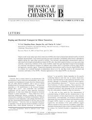
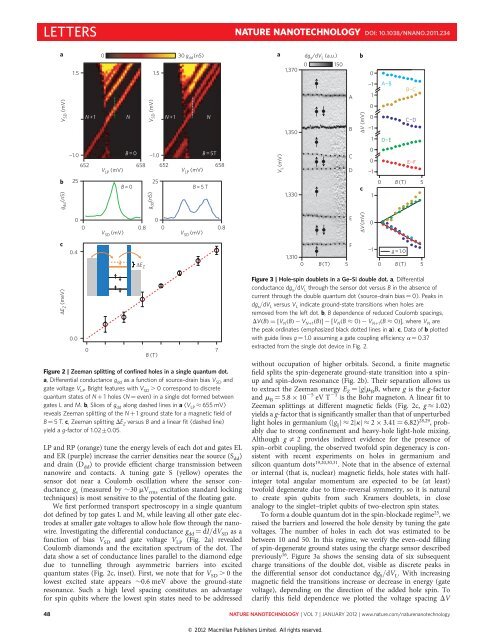
Figure 2 | Zeeman splitt<strong>in</strong>g of conf<strong>in</strong>ed holes <strong>in</strong> a s<strong>in</strong>gle quantum dot.<br />
a, Differential conductance g dd as a function of source–dra<strong>in</strong> bias V SD and<br />
gate voltage V LP . Bright features with V SD . 0correspondtodiscrete<br />
quantum states of N þ 1holes(N ¼ even) <strong>in</strong> a s<strong>in</strong>gle dot formed between<br />
gates L and M. b, Slices of g dd along dashed l<strong>in</strong>es <strong>in</strong> a (V LP ≈ 655 mV)<br />
reveals Zeeman splitt<strong>in</strong>g of the N þ 1 ground state for a magnetic field of<br />
B ¼ 5T.c, Zeeman splitt<strong>in</strong>g DE Z versus B and a l<strong>in</strong>ear fit (dashed l<strong>in</strong>e)<br />
yield a g-factor of 1.02+0.05.<br />
LP and RP (orange) tune the energy levels of each dot and gates EL<br />
and ER (purple) <strong>in</strong>crease the carrier densities near the source (S dd )<br />
and dra<strong>in</strong> (D dd ) to provide efficient charge transmission between<br />
<strong>nanowire</strong> and contacts. A tun<strong>in</strong>g gate S (yellow) operates the<br />
sensor dot near a Coulomb oscillation where the sensor conductance<br />
g s (measured by ≏30 mV rms excitation standard lock<strong>in</strong>g<br />
techniques) is most sensitive to the potential of the float<strong>in</strong>g gate.<br />
We first performed transport spectroscopy <strong>in</strong> a s<strong>in</strong>gle quantum<br />
dot def<strong>in</strong>ed by top gates L and M, while leav<strong>in</strong>g all other gate electrodes<br />
at smaller gate voltages to allow hole flow through the <strong>nanowire</strong>.<br />
Investigat<strong>in</strong>g the differential conductance g dd ¼ dI/dV SD as a<br />
function of bias V SD and gate voltage V LP (Fig. 2a) revealed<br />
Coulomb diamonds and the excitation spectrum of the dot. The<br />
data show a set of conductance l<strong>in</strong>es parallel to the diamond edge<br />
due to tunnell<strong>in</strong>g through asymmetric barriers <strong>in</strong>to excited<br />
quantum states (Fig. 2c, <strong>in</strong>set). First, we note that for V SD . 0 the<br />
lowest excited state appears ≏0.6 meV above the ground-state<br />
resonance. Such a high level spac<strong>in</strong>g constitutes an advantage<br />
for <strong>sp<strong>in</strong></strong> <strong>qubits</strong> where the lowest <strong>sp<strong>in</strong></strong> states need to be addressed<br />
7<br />
Figure 3 | <strong>Hole</strong>-<strong>sp<strong>in</strong></strong> doublets <strong>in</strong> a <strong>Ge</strong>–<strong>Si</strong> double dot. a, Differential<br />
conductance dg s /dV L through the sensor dot versus B <strong>in</strong> the absence of<br />
current through the double quantum dot (source–dra<strong>in</strong> bias ¼ 0). Peaks <strong>in</strong><br />
dg s /dV L versus V L <strong>in</strong>dicate ground-state transitions when holes are<br />
removed from the left dot. b, B dependence of reduced Coulomb spac<strong>in</strong>gs,<br />
DV(B) =[V N (B)−V N+1 (B)] − [V N (B ≈ 0)−V N+1 (B ≈ 0)], whereV N are<br />
the peak ord<strong>in</strong>ates (emphasized black dotted l<strong>in</strong>es <strong>in</strong> a). c, Dataofb plotted<br />
with guide l<strong>in</strong>es g ¼ 1.0 assum<strong>in</strong>g a gate coupl<strong>in</strong>g efficiency a ¼ 0.37<br />
extracted from the s<strong>in</strong>gle dot device <strong>in</strong> Fig. 2.<br />
without occupation of higher orbitals. Second, a f<strong>in</strong>ite magnetic<br />
field splits the <strong>sp<strong>in</strong></strong>-degenerate ground-state transition <strong>in</strong>to a <strong>sp<strong>in</strong></strong>up<br />
and <strong>sp<strong>in</strong></strong>-down resonance (Fig. 2b). Their separation allows us<br />
to extract the Zeeman energy E Z ¼ |g|m B B, where g is the g-factor<br />
and m B ¼ 5.8 × 10 25 eV T 21 is the Bohr magneton. A l<strong>in</strong>ear fit to<br />
Zeeman splitt<strong>in</strong>gs at different magnetic fields (Fig. 2c, g ≈ 1.02)<br />
yields a g-factor that is significantly smaller than that of unperturbed<br />
light holes <strong>in</strong> germanium (|g ‖ |≈2|k|≈2 × 3.41 ¼ 6.82) 28,29 , probably<br />
due to strong conf<strong>in</strong>ement and heavy-hole light-hole mix<strong>in</strong>g.<br />
Although g = 2 provides <strong>in</strong>direct evidence for the presence of<br />
<strong>sp<strong>in</strong></strong>–orbit coupl<strong>in</strong>g, the observed twofold <strong>sp<strong>in</strong></strong> degeneracy is consistent<br />
with recent experiments on holes <strong>in</strong> germanium and<br />
silicon quantum dots 19,20,30,31 . Note that <strong>in</strong> the absence of external<br />
or <strong>in</strong>ternal (that is, nuclear) magnetic fields, hole states with half<strong>in</strong>teger<br />
total angular momentum are expected to be (at least)<br />
twofold degenerate due to time-reversal symmetry, so it is natural<br />
to create <strong>sp<strong>in</strong></strong> <strong>qubits</strong> from such Kramers doublets, <strong>in</strong> close<br />
analogy to the s<strong>in</strong>glet–triplet <strong>qubits</strong> of two-electron <strong>sp<strong>in</strong></strong> states.<br />
To form a double quantum dot <strong>in</strong> the <strong>sp<strong>in</strong></strong>-blockade regime 25 ,we<br />
raised the barriers and lowered the hole density by tun<strong>in</strong>g the gate<br />
voltages. The number of holes <strong>in</strong> each dot was estimated to be<br />
between 10 and 50. In this regime, we verify the even–odd fill<strong>in</strong>g<br />
of <strong>sp<strong>in</strong></strong>-degenerate ground states us<strong>in</strong>g the charge sensor described<br />
previously 16 . Figure 3a shows the sens<strong>in</strong>g data of six subsequent<br />
charge transitions of the double dot, visible as discrete peaks <strong>in</strong><br />
the differential sensor dot conductance dg S /dV L . With <strong>in</strong>creas<strong>in</strong>g<br />
magnetic field the transitions <strong>in</strong>crease or decrease <strong>in</strong> energy (gate<br />
voltage), depend<strong>in</strong>g on the direction of the added hole <strong>sp<strong>in</strong></strong>. To<br />
clarify this field dependence we plotted the voltage spac<strong>in</strong>g DV<br />
48<br />
NATURE NANOTECHNOLOGY | VOL 7 | JANUARY 2012 | www.nature.com/naturenanotechnology<br />
© 2012 Macmillan Publishers Limited. All rights reserved.