LNBs for Satellite Broadcast - Sharp Global
LNBs for Satellite Broadcast - Sharp Global
LNBs for Satellite Broadcast - Sharp Global

You also want an ePaper? Increase the reach of your titles
YUMPU automatically turns print PDFs into web optimized ePapers that Google loves.
PCB<br />
ADVANCED FLEX PRINTED CIRCUIT BOARDS<br />
■ Advanced Flex Printed Circuit Boards <br />
The advanced flex printed circuit board is a multilayered wiring board comprising of flexible printed circuits (FPC) laminated into a<br />
multilayer configuration. The PWBs and FPCs are connected to each other via copper-plated through holes. It is ideal <strong>for</strong> compact,<br />
lightweight equipment design.<br />
◆ Features<br />
(1) For selecting optimal specifications to suit specific applications, special specifications such as <strong>for</strong> mobile phones are also available.<br />
• Minimum thickness in multi-layer part: 0.19 mm (4-layer), 0.33 mm (6-layer)<br />
• Minimum pattern width/pitch: 0.06/0.07 mm<br />
• Flexibility of single/double sided FPC part (dedicated <strong>for</strong> hinge): More than 200 000 times 180-degree bending of radius 3 mm<br />
(2) Capable of board-to-board connection without connectors, which enables space-saving and 3-dimensional equipment assembly.<br />
(3) Through hole plating connection of multi-layer (3 to 8) part to flexible part significantly improves reliability.<br />
(4) Blind Via Hole (BVH) <strong>for</strong>ming with laser via drilling of small diameter.<br />
(5) Sheet design provides excellent mountability, equivalent to that of PWB.<br />
◆ Outline Specifications<br />
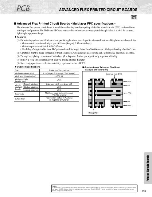
■ Construction of Advanced Flex Board<br />
(example of 6-layer BVH)<br />
Type Folding type/Flying tail type<br />
Min. base thickness (mm) 0.19 (4-layer), 0.33 (6-layer), 0.40 (8-layer)<br />
Min. line width/spacing (mm) 0.05/0.05<br />
Min. through hole<br />
diameter (mm)<br />
ø0.25<br />
Min. via<br />
Through hole (mm) Outer layer: ø0.5, Inner layer: ø0.5<br />
hole land Blind via hole (mm) ø0.09<br />
diameter<br />
Inner via hole (mm) ø0.30<br />
Solder resist<br />
Multi layer: Liquid photo solder resist,<br />
FPC: Film cover ray<br />
Surface finish<br />
Heat-resistant preflux, Ni-Au plating<br />
(Ni-Au plating <strong>for</strong> flying tail)<br />
Through hole<br />
Laser via hole (BVH)<br />
Notice<br />
In the absence of confirmation by device specification sheets, SHARP takes no responsibility <strong>for</strong> any defects that may occur in equipment<br />
using any SHARP devices shown in catalogs, data books, etc. Contact SHARP in order to obtain the latest device specification sheets<br />
be<strong>for</strong>e using any SHARP device.<br />
FPC<br />
PP<br />
FPC<br />
PP<br />
FPC<br />
103<br />
Printed Circuit Boards