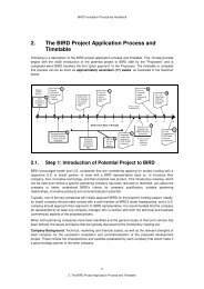
SemiconductorsWafer Defect Removal in Semiconductor ManufacturingThe CompaniesOrAmir Semiconductor Equipment Ltd. — Applied Materials, Inc.The Project06OrAmir was established in 1992 to utilize laser technology forsemiconductor applications. The company's roots andtechnology originated with RAFAEL, Israel's defensedevelopment organization. Prior to its acquisition by AppliedMaterials, OrAmir developed a dry, single step process solutionfor damage-free semiconductor wafer cleaning, based on aunique laser technology. This technology was targeted forsingle-step dry photo resist stripping in semiconductor wafermanufacturing. Leading edge semiconductor manufacturersthroughout the world, as well as organizations such asSEMATECH (USA) and ASET (Japan) have tested OrAmir'sprocess and have acknowledged that it is complete, effectiveand damage-free.Applied Materials, a Fortune 500 Global Growth Company,is the largest supplier of products and services to the globalsemiconductor industry. Applied Materials manufacturessystems that perform chemical and physical vapor deposition,epitaxial and polysilicon deposition, rapid thermal processing,plasma etching, ion implantation, metrology, inspection andchemical mechanical polishing. Applied Materials maintainsresearch, development and manufacturing centers in the U.S.,Israel, Europe and Japan, as well as technology centers inSouth Korea and Taiwan. More than a year ago, AppliedMaterials acquired OrAmir and has integrated it to become akey product unit of the company.In the last few years, cleaning of particles and defects hasbecome a much more challenging process for thesemiconductor industry, and there are a variety of techniquesbeing developed to help increase its effectiveness. In addition,customers are realizing that the role of inspection, onceconsidered a non-added-value necessity, has become muchmore important and are willing to substantially invest more inorder to improve the manufacturing process.These two trends provide the driving force for combining theadvanced inspection capabilities of Applied Materials andOrAmir's unique laser cleaning process into an integratedinspection cleaning concept. By combining the capabilitiesof inspection at Applied Materials, with the selective cleaningprocess from OrAmir, the resulting synergy of the two systemshas led to a unique and innovative solution for an urgentindustry problem.The <strong>BIRD</strong> project between Applied Materials and OrAmir,initiated at the beginning of 2000, led to the development ofa state-of-the-art laser cleaning system capable of effectivelyremoving defects from the most demanding applications inthe semiconductor area. The fully manufacturable systemmeets the strict standards of the semiconductor industry andis currently being field-tested at some of the most sophisticated,high-end customers in the world.Through the <strong>BIRD</strong>-funded collaboration, the relationshipbetween the two companies continued to develop, ultimatelyleading to the full acquisition of OrAmir by Applied in June2001, just 18 months following the initiation of the project.
“I believe that the <strong>BIRD</strong> <strong>Foundation</strong> played an important role”in bringing Applied Materials and OrAmir together through asuccessful joint development program that ultimately led tothe acquisition of OrAmir by Applied Materials.Dan MaydanPresident, Applied MaterialsCompetitive manufacturing process foradvanced semiconductor devicesDan Maydan President, Applied MaterialsMinimizes unseen defectsImproves final waferand device yieldsIntegration of a small wafer-cleaningmodule in a sophisticated inspection toolSelective treatment ofcontaminated locationsInspection tool identifies defect locations07