Si3217x Si3291x
Si3217x Si3291x
Si3217x Si3291x
- No tags were found...

You also want an ePaper? Increase the reach of your titles
YUMPU automatically turns print PDFs into web optimized ePapers that Google loves.
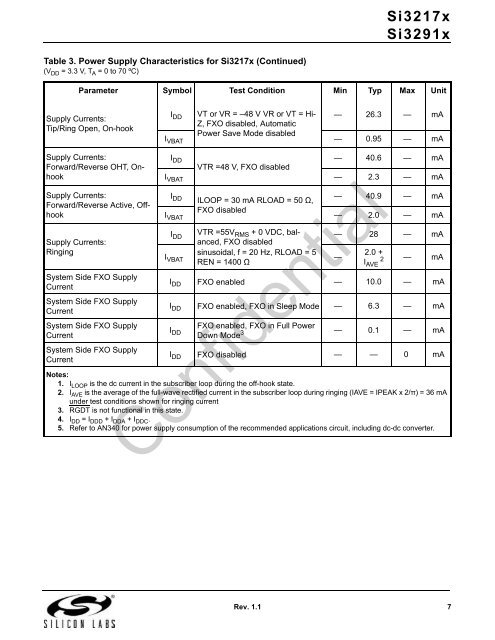
<strong>Si3217x</strong><strong>Si3291x</strong>Table 3. Power Supply Characteristics for <strong>Si3217x</strong> (Continued)(V DD =3.3V, T A = 0 to 70 ºC)Parameter Symbol Test Condition Min Typ Max UnitSupply Currents:Tip/Ring Open, On-hookSupply Currents:Forward/Reverse OHT, OnhookSupply Currents:Forward/Reverse Active, OffhookSupply Currents:RingingSystem Side FXO SupplyCurrentSystem Side FXO SupplyCurrentSystem Side FXO SupplyCurrentSystem Side FXO SupplyCurrentI DD VT or VR = –48 V VR or VT = Hi- — 26.3 — mAZ, FXO disabled, AutomaticI VBATPower Save Mode disabled— 0.95 — mAI DD— 40.6 — mAVTR =48 V, FXO disabledI VBAT — 2.3 — mAI DD ILOOP = 30 mA RLOAD = 50 Ω,— 40.9 — mAI VBATFXO disabled— 2.0 — mAI DDVTR =55V RMS + 0 VDC, balanced,FXO disabledsinusoidal, f = 20 Hz, RLOAD = 5I VBAT —REN = 1400 Ω— 28 — mA2.0 +I AVE2 — mAI DD FXO enabled — 10.0 — mAI DD FXO enabled, FXO in Sleep Mode — 6.3 — mAI DDFXO enabled, FXO in Full PowerDown Mode 3 — 0.1 — mAI DD FXO disabled — — 0 mANotes:1. I LOOP is the dc current in the subscriber loop during the off-hook state.2. I AVE is the average of the full-wave rectified current in the subscriber loop during ringing (IAVE = IPEAK x 2/π) = 36 mAunder test conditions shown for ringing current3. RGDT is not functional in this state.4. I DD =I DDD +I DDA +I DDC .5. Refer to AN340 for power supply consumption of the recommended applications circuit, including dc-dc converter.Rev. 1.1 7