Volume 11 Issue 2 - STI Electronics, Inc.
Volume 11 Issue 2 - STI Electronics, Inc.
Volume 11 Issue 2 - STI Electronics, Inc.
- No tags were found...

Create successful ePaper yourself
Turn your PDF publications into a flip-book with our unique Google optimized e-Paper software.
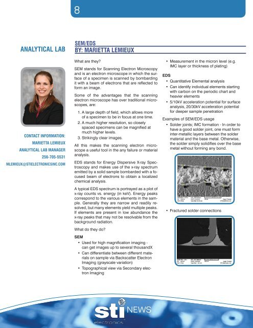
8Analytical labContact Information:marietta lemieuxanalytical lab manager256-705-5531mlemieux@stielectronicsinc.comSEM/EDSBY: Marietta LemieuxWhat are they?SEM stands for Scanning Electron Microscopyand is an electron microscope in which the surfaceof a specimen is scanned by bombardingit with a beam of electrons that are reflected toform an image.Some of the advantages that the scanningelectron microscope has over traditional microscopes,are:1. A large depth of field, which allows moreof a specimen to be in focus at one time.2. A much higher resolution, so closelyspaced specimens can be magnified atmuch higher levels.3. Strikingly clear images.All this makes the scanning electron microscopea useful tool in the any failure or materialanalysis.EDS stands for Energy Dispersive X-ray Spectroscopyand makes use of the x-ray spectrumemitted by a solid sample bombarded with a focusedbeam of electrons to obtain a localizedchemical analysis.A typical EDS spectrum is portrayed as a plot ofx-ray counts vs. energy (in keV). Energy peakscorrespond to the various elements in the sample.Generally they are narrow and readily resolved,but many elements yield multiple peaks.If elements are present in low abundance thex-ray peaks that may not be resolvable from thebackground radiation.What do they do?SEM• Used for high magnification imaging -can get images up to several thousandX• Can differentiate between different materialson sample via Backscatter ElectronImaging (grayscale variation)• Topographical view via Secondary electronImaging• Measurement in the micron level (e.g.IMC layer or thickness of plating)EDS• Quantitative Elemental analysis• Can identify individual elements startingwith carbon on the periodic chart andheavier elements• 5/10kV acceleration potential for surfaceanalysis, 20/30kV acceleration potentialfor deeper sample penetrationExamples of SEM/EDS usage• Solder joints; IMC formation - In order tohave a good solder joint, one must forminter-metallic layers between the soldermaterial and the base metal. Otherwise,the solder simply solidifies over the basemetal without forming any bond.• Fractured solder connectionsNEWS