

WARNING!
EPE 2004-06
EPE 2004-06
- No tags were found...

You also want an ePaper? Increase the reach of your titles
YUMPU automatically turns print PDFs into web optimized ePapers that Google loves.
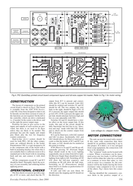
Fig.4. PIC QuickStep printed circuit board component layout and full-size copper foil master. Refer to Fig.1 for motor wiring.<br />
CONSTRUCTION<br />
The layout of components on the printed<br />
circuit board is shown in Fig.4. This board<br />
is available from the EPE PCB Service,<br />
code 448. It has been designed so that it can<br />
be literally cut into three sections if some of<br />
the functions are not required. On the left is<br />
the controller, which can drive a dedicated<br />
i.c. if needed. In the centre is the driver, and<br />
on the right the power output stage.<br />
Positions for pins to give access to the<br />
inputs and outputs of each section are provided,<br />
but there is no need to fit these<br />
unless they are likely to be needed. The<br />
prototype has just the supply and output<br />
pins fitted, plus the two for frequency<br />
counter connection.<br />
Dual-in-line (d.i.l.) sockets should be<br />
used for both PICs. All the other components<br />
are soldered directly to the board.<br />
Potentiometer VR1 is a type designed to fit<br />
to the component side of the board with a<br />
built-in mounting bracket, but where this is<br />
not available there is sufficient room to fit a<br />
standard pot to the board with its mounting<br />
bush and nut, and connect it with short<br />
leads.<br />
All the components except IC1 and IC2<br />
should be fitted. Throughly check the accuracy<br />
of your assembly and soldering before<br />
applying power.<br />
OPERATIONAL CHECKS<br />
The first check is to power up with a supply<br />
of 6V or more, and check that the 5V<br />
output from IC3 is present and correct.<br />
After this IC1 can be inserted. Link LK1<br />
should be omitted and switches S1 and S2<br />
should be off. The two outputs, the wire<br />
links to the right, should be high (+5V). If<br />
S5 is pressed, the upper output link should<br />
go low (0V). If S6 is pressed, the upper output<br />
link should alternate between high and<br />
low at a rate adjustable with VR1.<br />
Switches S4 and S3 should have a similar<br />
effect on the lower output link. If this<br />
works, this part of the circuit should be<br />
fully functional, but feel free to try “direction<br />
and step” mode with link LK1 fitted,<br />
and to check out the counter output from<br />
TP1 if desired.<br />
IC2 can be fitted next, with LK2 omitted<br />
and LK3 in place. Incidentally, LK1 and<br />
LK2 should always be fitted or removed as<br />
a pair so that the modes of IC1 and IC2 are<br />
the same, so LK1 should also be omitted at<br />
this point in testing.<br />
If S9 (Wave) is on and S7 and S8 are off,<br />
repeatedly pressing S5 (Forward Single<br />
Step) should result in the l.e.d.s lighting<br />
sequentially, one at a time from left to right.<br />
S4 (Reverse Single Step) should have them<br />
lighting from right to left. Switching off S9<br />
will show the full-step sequence, and<br />
switching on S8 will show the half steps.<br />
Switching on S7 (Powerdown) should<br />
show brief l.e.d. flashes as pushswitches S3<br />
to S6 are pressed.<br />
If LK1 and LK2 are now fitted, S4<br />
should cause the stepping and S5 should set<br />
the direction.<br />
Low voltage d.c. stepper motor.<br />
MOTOR CONNECTIONS<br />
The unit can now be tested with a motor!<br />
If this came with connection data there<br />
should be no problem connecting it up to<br />
this project. If it didn’t, or it was salvaged<br />
from scrap equipment, the connections will<br />
have to be identified.<br />
The “common” leads can be located with<br />
a meter. Where a resistance can be measured<br />
across any two leads, it will be found<br />
that it will be either the value for a coil lead<br />
to a common, or twice that value, i.e. two<br />
coils in series via a common. So, the common(s)<br />
will be the lead(s) having the lower<br />
resistance value compared to two or more<br />
of the others. Fig.1 shows how this comes<br />
about.<br />
Having identified the common(s), connect<br />
them to the positive output of a<br />
Everyday Practical Electronics, June 2004 379