helmholTz-zenTrum Berlin (hzB) - EXPO21XX.com
helmholTz-zenTrum Berlin (hzB) - EXPO21XX.com
helmholTz-zenTrum Berlin (hzB) - EXPO21XX.com

You also want an ePaper? Increase the reach of your titles
YUMPU automatically turns print PDFs into web optimized ePapers that Google loves.
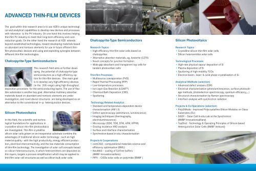
AdvAnced Thin-Film devices<br />
The goal within this research area is to use HZB‘s unique technological<br />
and analytical capabilities to develop new devices and processes<br />
with relevance to the PV industry. On one hand this involves helping<br />
thin-fi lm PV industry to meet their long-term effi ciency and costreduction<br />
goals. On the other hand the research at HZB extends<br />
beyond established technologies, toward developing materials based<br />
on abundant and nontoxic elements for use in future effi cient thinfi<br />
lm photovoltaic devices and using and exploiting synergies between<br />
different thin-fi lm technologies.<br />
chalcopyrite-Type semiconductors<br />
This research fi eld aims at further developing<br />
the potential of chalcopyrite-type<br />
semiconductors as a high effi ciency option<br />
for thin-fi lm devices. One main goal<br />
is to develop very high-effi ciency devices<br />
(in the 20% range) using high-throughput<br />
deposition processes for the semiconducting layers. The use of fl exible<br />
substrates is another key goal. Alternative multinary absorber<br />
materials based on abundant and nontoxic elements are under<br />
investigation, and novel device structures are being developed as an<br />
alternative to the conventional n+-p heterojunction devices.<br />
silicon Photovoltaics<br />
In this fi eld, the scientifi c and technological<br />
foundations for applications in<br />
crystalline silicon thin-fi lm photovoltaics<br />
are investigated. Thin-fi lm crystalline<br />
silicon solar cells grown on an inexpensive substrate <strong>com</strong>bine the<br />
advantages of traditional silicon wafer technology - such as high<br />
material quality - with the high productivity, energy effi cient production,<br />
electrical interconnectivity, and the low materials consumption<br />
of thin-fi lm technology. The investigation of solar cell concepts based<br />
on silicon heterostructures, in which heteroemitters are deposited as<br />
thin layers, targets a process simplifi cation which may be applied to<br />
thin-fi lm solar cell structures as well as silicon bulk solar cells.<br />
chalcopyrite-Type semiconductors<br />
Research Topics<br />
• High-effi ciency thin-fi lm solar cells based on<br />
chalcopyrites<br />
• Alternative absorber materials, eg. kesterite (CZTS)<br />
• Novel concepts for junction formation<br />
• Wide-gap absorbers and transparent top cells for<br />
tandem photovoltaic cells<br />
Thin-fi lm Processes<br />
• Multisource coevaporation (PVD)<br />
• Rapid Thermal Processing (RTP)<br />
• Low-temperature processes<br />
• Ion Layer Gas Reaction (ILGAR TM )<br />
• Chemical Bath Deposition (CBD)<br />
• Sputtering<br />
Technology Related Analytics<br />
• Standard and temperature-dependent device<br />
characterisation (AM1.5)<br />
• Defect spectroscopy (admittance, luminescence)<br />
• Imaging techniques (thermography,<br />
electroluminescence)<br />
• Microscopy (SEM, TEM, STM, AFM, KPFM)<br />
• Grazing incidence XRD analysis<br />
• Surface and interface characterisation<br />
• Synchrotron-based in-situ characterisation<br />
Projects & Cooperations<br />
• <strong>com</strong>CIGS - <strong>com</strong>putational materials science and<br />
effi ciency optimisation (BMU)<br />
• NeuMAS – scaling of Cd-free buffers<br />
(BMBF Innovations allianz)<br />
• PIPV – CIGSe solar cells on polyimide (BMBF )<br />
silicon Photovoltaics<br />
Research Topics<br />
• Crystalline silicon thin-fi lm solar cells<br />
• Silicon heteroemitter solar cells<br />
Technological Processes<br />
• High-rate physical vapour deposition of Si<br />
• Plasma deposition of Si<br />
• Sputtering of high-mobility TCOs<br />
• Electron-beam-, laser- & solid phase crystallisation of Si<br />
Analytical Methods (selection)<br />
• Advanced defect analysis (ESR)<br />
• Electrical characterisation (photoluminescence, surface photovoltage<br />
methods, photoelectron spectroscopy, quantum effi ciency,…)<br />
• Structural characterisation by Raman spectroscopy<br />
• Interface analysis with synchrotron radiation<br />
Projects & Co-Operations (selection)<br />
• PolySiMode - Improved Polycrystalline-Silicon Modules on Glass<br />
Substrates (EU)<br />
• SISSY – Solar Cell In-situ Lab at the Synchrotron<br />
(BMBF Innovations allianz)<br />
• TopShot - Technology & Operating Principles of Silicon-based<br />
Heterojunction Solar Cells (BMBF Verbund)