LU-QORF_2017

Create successful ePaper yourself
Turn your PDF publications into a flip-book with our unique Google optimized e-Paper software.
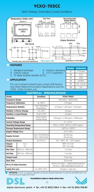
VCXO-705CC<br />
SMD Voltage Controlled Crystal Oscillators<br />
Dimensions (Units: mm)<br />
Top View<br />
Recommended<br />
Solder Pattern<br />
Test Circuit<br />
Output Waveform<br />
FEATURES<br />
7.0 x 5.0 x 1.8<br />
1. Miniature package. 4. Industry standard.<br />
2. CMOS output. 5. 3.3 V operation.<br />
3. Tri-State enable/disable (E/D).<br />
APPLICATION<br />
For use in phase locked loops, phase shift keying<br />
and other telecommunication applications such as<br />
ADSL, Cable modem, etc.<br />
ELECTRICAL SPECIFICATIONS<br />
Model Condition VCXO-705CC<br />
Frequency Range<br />
All specifications subject to change without notice.<br />
73<br />
Terminal Connection<br />
#1 V Control<br />
#2 E/D<br />
#3 GND<br />
#4 OUTPUT<br />
#5 N.C. or E/D<br />
#6 VDD<br />
50.0 MHz ~200.0 MHz<br />
Frequency Calibration at +25°C ±15 ppm<br />
Temperature Stability<br />
Over Operating<br />
Temperature<br />
±15 ppm / ±25 ppm / ±50 ppm<br />
Stability vs Power Change VDD ±5% ±5 ppm<br />
Stability vs Load Change 15 pF ±10% ±3 ppm<br />
Pullability<br />
Over Control<br />
Voltage Range<br />
±50 ppm / ±100 ppm / ±200 ppm<br />
Control Voltage Range<br />
0 ~ 3.3 V<br />
Operating Temperature Range<br />
0°C to +70°C, -40°C to +85°C option<br />
Storage Temperature Range<br />
-55°C to +125°C<br />
Supply Voltage (VDD) 3.3 V ±5%<br />
Supply Current<br />
50.0~95.999 MHz<br />
96.0~200.0 MHz<br />
30 mA max.<br />
40 mA max.<br />
Output Symmetry at 1/2 VDD 40 ~ 60%, 45 ~ 55% option<br />
Output<br />
Voltage<br />
**Includes stray and probe capacitance<br />
VOH<br />
VOL<br />
90% VDD min.<br />
10% VDD max.<br />
Rise Time 20% VDD ~ 80% VDD 1 ns max.<br />
Fall Time 80% VDD ~ 20% VDD 1 ns max.<br />
Symmetry=T1/T0x100%<br />
Output Load<br />
15 pF max.<br />
Start Time<br />
10 ms max.<br />
Pin 2, Tri-State Function<br />
Pin 2= H or open ... output active at pin 4,5<br />
Pin 2= L ...high impendance at pin 4,5<br />
Aging first year at +25°C ±3°C ±2 ppm / year max.<br />
OPTIONS: A 0.01 uF bypass capacitor should be placed between VDD (pin 6) and GND (pin 3) to<br />
minimize power supply line noise.<br />
digital electronic gmbh • Tel.: +49 (0) 8221/708-0 • Fax: +49 (0) 8221/708-80