


Create successful ePaper yourself
Turn your PDF publications into a flip-book with our unique Google optimized e-Paper software.
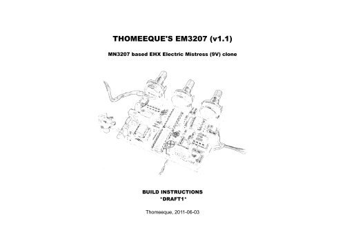
THOMEEQUE'S EM3207 (<strong>v1.1</strong>)<br />
MN3207 based EHX <strong>Electric</strong> Mistress (9V) clone<br />
BUILD INSTRUCTIONS<br />
*DRAFT1*<br />
Thomeeque, 2011-06-03
THOMEEQUE'S EM3207 (<strong>v1.1</strong>) BUILD INSTRUCTIONS *DRAFT1* 2 / 6<br />
INTRODUCTION<br />
EM3207 is a loose clone of the original 9V EHX <strong>Electric</strong> Mistress chorus/flanger<br />
adapted for MN3207 BBD chip.<br />
Additionally it features:<br />
• Unity gain (no volume drop compared to true-bypass) without need of additional<br />
amplification,<br />
• Input RF filter to avoid interferences between internal clock and AM radio<br />
rubbish picked from the air,<br />
• Improved VCC filtering for LFO section to lower danger of LFO ticking leaking<br />
into the audio signal via supply tracks.<br />
BUILD NOTES<br />
1. Use sockets for all ICs as layout expects it, precise type.<br />
2. Solder all direct jumpers first, some of them start/end under IC sockets, it would be<br />
problematic to install them if sockets were already there.<br />
3. Next solder all laying diodes and resistors, then sockets, then small caps etc.<br />
Simply go from the lowest to the highest components.<br />
4. Long jumpers (feedback jumper and clock jumpers) solder when all parts are<br />
placed on the PCB (twist clock jumpers together and lead them shortest possible<br />
way - you can switch them, it does not matter which one ends at CP1 and which<br />
one at CP2).<br />
5. FLAGE / FILTER-MATRIX mode switch (SW_MODE) is wired off-board, see<br />
schematic.<br />
6. Rest of off-board wiring (IN/OUT jacks, switching, DC jack etc.) is not covered by<br />
this document, usual true-bypass switching and stompbox wiring is expected.<br />
7. It can be problematic to get 1M/EXP (reverse-audio) potentiometer for<br />
POT2_RATE, I usually use 1M/LOG (audio) pot with reversed function in these<br />
situations instead. PCB therefor leaves middle lug of this pot unconnected to be<br />
ready for both scenarios. Jumper must be soldered to connect pot's middle lug with<br />
one of outer lugs, depending on the pot type (as indicated on the layout pictures).<br />
8. If wiring potentiometers off-board, keep leads to them as short as possible,<br />
especially those leading to the RATE pot generate lot of electromagnetic hum. For<br />
the same reason try to lead audio signal wires and place IN/OUT jacks as far from<br />
LFO&Clock circuitry as possible. If you still get ticking into the signal, you can try<br />
to introduce some shielding there.<br />
9. Between power pins of each of ICs should be at the bottom (solder) side of PCB<br />
soldered 100nF ceramic filtering capacitor (not drawn on schematics) for enhanced<br />
VCC filtering.<br />
10. Do as many partial checks as possible (layout is very tight and circuitry has already<br />
some level of complexity, so try to avoid potential future debugging until it's easy<br />
yet):<br />
• Check new etched PCB traces for cuts and bleeds,<br />
• Check that all direct jumpers are there before proceeding with soldering of the<br />
components,<br />
• Check all resistor values by DMM before soldering,<br />
• Double-check orientation of IC sockets before soldering (and of ICs<br />
themselves later before putting them in of course),<br />
• Double-check polarity of all polarized caps before soldering,<br />
• Double-check right pinout of transistors before soldering,<br />
• Basically double-check every component and every wire (right position, right<br />
value, right orientation) before soldering,<br />
• When all parts and jumpers are soldered and you are about to start putting the<br />
real ICs there for the first time, check yet before that expected voltages<br />
(especially GND and VCC) are at expected pins of all IC sockets (and vice<br />
versa).<br />
• Don't put all ICs there at once, fill them by functional blocks (LFO, clock,<br />
input buffer, BBD..) and check that given block works before filling another<br />
one.<br />
11. VCC = 10V max. (MN3207 limitation)<br />
ALIGNMENT PROCEDURE<br />
• TODO<br />
ADVICED MODS<br />
• Play with C4 (feedback cap) value to get your own COLOR.<br />
• Play with C7 and C8 values to get darker or brighter wet signal character.<br />
• Play with C17 (clock cap) to move wet signal delay range (bigger value will move<br />
you to darker flanger and more to chorus area). You may install SPDT on-off-on<br />
switch adding e.g. 22pF and 68pF caps in parallel to C17 (use CC wirepads).<br />
• To adjust overall gain play with R5 value (A = 1 + R5/R4), but note that bigger<br />
gain at this point leads to lower dynamic range – use it only to get real unity gain,<br />
if default value does not work for you.
THOMEEQUE'S EM3207 (<strong>v1.1</strong>) BUILD INSTRUCTIONS *DRAFT1* 3 / 6<br />
SCHEMATIC
THOMEEQUE'S EM3207 (<strong>v1.1</strong>) BUILD INSTRUCTIONS *DRAFT1* 4 / 6<br />
PCB 1:1 (NORMAL / MIRRORED), LAYOUT (WIREPADS & JUMPERS)
THOMEEQUE'S EM3207 (<strong>v1.1</strong>) BUILD INSTRUCTIONS *DRAFT1* 5 / 6<br />
LAYOUT (NAMES / VALUES)
THOMEEQUE'S EM3207 (<strong>v1.1</strong>) BUILD INSTRUCTIONS *DRAFT1* 6 / 6<br />
PART LIST<br />
Note: All capacitors rated 16V or more<br />
Resistors:<br />
1x 10R (R35)<br />
1x 47R (R36)<br />
2x 470R (R6, R17)<br />
1x 510R (R19)<br />
2x 1k (R11, R20)<br />
1x 3k6 (R5)<br />
2x 3k9 (R25, R33)<br />
3x 4k7 (R8, R12, R13)<br />
1x 5k6 (R9)<br />
1x 8k2 (R21)<br />
6x 10k (R4, R15, R16, R18, R26, R34)<br />
1x 14k (R10)<br />
1x 24k (R22)<br />
1x 27k (R27)<br />
1x 30k (R24)<br />
1x 33k (R30)<br />
2x 39k (R23, R29)<br />
2x 47k (R14, R28)<br />
1x 62k (R32)<br />
2x 100k (R2, R7)<br />
1x 1M (R3)<br />
1x 1M2 (R31)<br />
1x 2M2 (R1)<br />
Resistor Trimmers (Cermet T93YB):<br />
1x 10k (RT1)<br />
1x 22k (RT3)<br />
1x 100k (RT2) Precise multi-turn type<br />
Disc (Ceramic) Capacitors:<br />
1x 22p (C17) Clock cap<br />
1x 150p (C1) RF filter<br />
6x 100n - IC GND-VCC filtering, see build note 9.<br />
Foil Capacitors (RM5):<br />
1x 680p (C7)<br />
1x 1n (C5)<br />
1x 2n2 (C4) Feedback cap<br />
1x 10n (C2)<br />
3x 47n (C3, C9, C11)<br />
1x 82n (C8)<br />
1x 220n (C10)<br />
Tantal Capacitors:<br />
2x 1μ (C15, C16)<br />
1x 4μ7 (C6)<br />
1x 10μ (C12)<br />
2x 33μ (C13, C14)<br />
Elyt Capacitors:<br />
3x 220μ (C18, C19, C20)<br />
Diodes:<br />
1x 1N4001 (D1)<br />
1x 1N4148 (D2)<br />
1x Zenner 10V/5W (D3)<br />
Transistors:<br />
1x 2N3904 (Q1)<br />
1x 2N5087 (Q2)<br />
ICs + sockets:<br />
1x CD4013B (IC5, DIL14)<br />
1x CD4049B (IC6, DIL16)<br />
1x JRC4558 (IC1, DIL8)<br />
1x LM311N (IC4, DIL8)<br />
1x LM324 (IC3, DIL14)<br />
1x MN3207 (IC2, DIL8)<br />
Potentiometers:<br />
1x 100k/LIN (POT3_RANGE)<br />
1x 10k/LIN (POT1_COLOR)<br />
1x 1M/EXP (POT2_RATE) EXP = reverse-audio, see build note 7.<br />
Switches:<br />
1x DPDT Toggle (SW_MODE)