ORION: 3D Geometry Measurement and NIR Inspection ... - intego.de
ORION: 3D Geometry Measurement and NIR Inspection ... - intego.de
ORION: 3D Geometry Measurement and NIR Inspection ... - intego.de

Create successful ePaper yourself
Turn your PDF publications into a flip-book with our unique Google optimized e-Paper software.
<strong>ORION</strong>: <strong>3D</strong> <strong>Geometry</strong> <strong>Measurement</strong><br />
<strong>and</strong> <strong>NIR</strong> <strong>Inspection</strong> of Silicon Blocks<br />
Area of application<br />
In the manufacturing of solar cells <strong>and</strong> modules<br />
one has a variety of different high ad<strong>de</strong>d value<br />
production steps. It is therefore reasonable to sort out<br />
faulty parts as soon as possible or even better to<br />
avoid processing them.<br />
From the silicon raw material one grows a crystal<br />
ingot which is then sawed (b<strong>and</strong> or wire) into the<br />
silicon blocks. After the block squaring follows<br />
a polishing step which gives the block the correct<br />
geometry for later processing (wafer sawing) <strong>and</strong><br />
reduces induced stress from the squaring.<br />
The <strong>3D</strong> geometry measurement is located after<br />
the squaring process generating proposals for the<br />
polishing system to reduce the polishing effort.<br />
Depending of the surface quality (see technical<br />
data), the <strong>NIR</strong> inspection can be combined with the<br />
<strong>3D</strong> geometry measurement or must be <strong>de</strong>signed as<br />
a separate system after the polishing step, where<br />
the block shows a clean smooth surface. The <strong>NIR</strong><br />
inspection then generates cutting proposals for the<br />
wafer sawing process.<br />
The blue regions are<br />
a <strong>3D</strong> reconstruction<br />
of SiN <strong>and</strong> SiC<br />
impurities in a<br />
silicon block due to<br />
contaminations in<br />
the crystal growth<br />
process. These<br />
regions shall not<br />
be processed further.<br />
Our silicon block inspection systems offer a fully<br />
automated solution for the inspection task before the<br />
two process steps polishing <strong>and</strong> wafer sawing.<br />
Preconditions for <strong>de</strong>ployment<br />
The automatic inspection of silicon blocks is suitable<br />
for continuous automated production as well as for<br />
manual operation as a st<strong>and</strong>-alone system, e.g. for<br />
the laboratory.<br />
A cleaning station can be integrated to assure the<br />
purification of the block surface, e.g. to clean the<br />
residues from the polishing. Consequently, high<br />
pseudo-error rates caused by surface impurities are<br />
averted.<br />
The optical probes incorporated in the inspection<br />
system are mostly housed to compensate for any<br />
variations in ambient lighting. As a result, no<br />
restrictions need to be ma<strong>de</strong> on the environmental<br />
lighting conditions.<br />
The inspection system will be <strong>de</strong>livered with a<br />
complete internal transfer system. One si<strong>de</strong> of the<br />
system is reserved for the loading <strong>and</strong> unloading. The<br />
supply can there either be managed by h<strong>and</strong> or by<br />
an automatic system integrated into the production.<br />
Contact<br />
Intego GmbH<br />
Henri-Dunant-Straße 8<br />
D-91058 Erlangen<br />
Fon +49 9131 61082-0<br />
Fax +49 9131 61082-999<br />
Email info@<strong>intego</strong>.<strong>de</strong><br />
Web www.<strong>intego</strong>.<strong>de</strong><br />
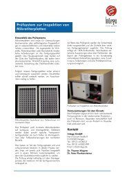
Our silicon<br />
blocks inspection<br />
system covers<br />
both the <strong>3D</strong><br />
geometry<br />
measurement<br />
<strong>and</strong> the <strong>NIR</strong><br />
inspection for<br />
inclusions in<br />
examination<br />
cycles of some<br />
minutes<br />
per block.