EPP Europe P1.2020
- Text
- Assuraance
- Test
- Production
- Assembly
- Packaging
- Printing
- Process
- Technologies
- Automation
- Manufacturing
PCB + ASSEMBLY In-lab
PCB + ASSEMBLY In-lab testing helps match the best cleaning fluid to the PCB contaminants. Test-cleaning in small batches prior to full-scale manufacturing can be beneficial to achieving a successfully functioning part. Once the cleaning fluid and process have been demonstrated to work on a smaller scale, production can be increased to the higher volumes required. Through small-batch preemptive testing, any elements of surprise are eliminated to ensure better board reliability. Pre-testing can take place in-house if a facility has the correct capabilities, however, out-sourcing is a popular choice for the assurance of PCB cleanliness. Specialist companies can undertake comprehensive testing and cleaning trials, which adhere to the standards specified by the PCB designer. This can be anything from simple visual testing to strict IPC-610 requirement testing. Visual inspection looks for any apparent flux material or white residue left behind after production. With no quantitative results, it is an important method to use alongside other processes, particularly in high-reliability electronics manufacturing. If precision is critical, for example in the medical industry, stringent testing must be completed. This can include methods like Surface Insulation Resistance testing (SIR) which focuses on determining the reliability of an electrical component based on the strength and quality of the signal that comes through the component after cleaning. Another technique is Ion Chromatography (IC) testing. This is the only test that detects and quantifies weak organic acids and individual ions. It is an excellent process to quickly troubleshoot the source of contamination and predict the effect of each ionic type. Critical cleaning testing like SIR and IC are usually undertaken in critical cleaning labs. Sample parts are methodically tested to ensure cleaning success. Results are verified and documented to validate the cleaning process. Recommendations are then made confirming the cleaning fluid and process that will work effectively when full-scale production commences. Source: MicroCare Corporation Call in the cleaning experts To ensure cleanliness designers should consult with a critical cleaning partner that specialises in collaboration and cooperative problem-solving. Carrying out cleaning trials on PCBs that use the industry’s leading flux and solder pastes takes place daily within these dedicated critical cleaning labs. This means specific cleaning fluids and processes can be easily identified to successfully clean the PCB and ensure its reliability. A service like this will have substantial benefits to the bottom-line if applied during the planning process. Before out-sourcing any cleaning tests, there are a few fundamentals to look for when choosing a critical cleaning partner. • Do they have the technical expertise? Can they offer specific advice on cleaning a diverse range of PCB substrates through the use of different cleaning methods? There is no one size fits all when it comes to cleaning PCBs, so cleaning tests are essential. These can be performed through on-site cleaning audits or in a critical cleaning lab. Both methods will determine the contamination and what cleaning fluid and process will work effectively. • Pre-testing may have been undertaken in the early design stages, which has led to the correct cleaning process, however, testing should be ongoing. Choose a vendor that supports PCB designers throughout each phase of the process from research and design to testing and manufacturing and can respond quickly to change. This will help to identify any issues before they become critical. • Seriously consider testing in a critical cleaning lab. It is here where cleaning tests are conducted to match the cleaning fluid to the flux and paste contaminants. This ensures the PCBs are clean and will function properly. Small batch preemptive test cleaning helps eliminate any surprises. Plan, plan, plan Early planning is key to the successful production of electronic products, particularly when it comes to cleaning. Designers must put cleanliness at the top of the agenda when designing a PCB, this will help to ensure long-term PCB performance, functionality and reliability. Initiating pre-testing and through the selection of cleaning fluids and methods in the initial design stage will help to resolve cleaning problems before manufacturing begins reducing rework and discarded boards. Partner with a cleaning expert to quickly and effectively identify the best cleaning methods and fluids for the job. The long-term benefits will be substantial when it comes to time, finances and the successful production of a fail-safe product. www.microcare.com Source: MicroCare Corporation 32 EPP EUROPE April 2020
PRODUCT UPDATES PCB + ASSEMBLY In use intelligent factory measurement tool Source: Insituware The Vision product family consists of the Mark-1 handheld device, the plug and play modules, application programs, and the Insitucloud. The handheld Mark-1 solution comes with Vision Insight, which enables the non-destructive inspection and process control of materials. Source: Insituware Insituware integrates hardware and software technology to assess materials during use. They combine analytical sensors, smart devices, and intelligent cloud-based information with innovative packaging methods to enable nonintrusive sensing of materials in motion. The company is cloud-based and operates with materials-specific apps on a handheld device. This enables better control by assessing materials on location and during use or in situ meaning ‘in place’. With analytical sensors, smart devices, and intelligent cloudbased information with innovative packaging methods, the company enables nonintrusive sensing. Measuring “in situ” (i.e. while in use) provides benefits over lab measurements, including: Effective: Enables users to make decisions quickly. Inexpensive: Integrated analytical sensors can be deployed at scale. Quick: Automated interpretations generated using machine learning methods. Intelligent factory measurement The Vision product family consists of the Mark-1 handheld device, the plug and play modules, material specific Mark-1 application programs (“Apps”), and the Insitucloud which incorporates the data management system, “MethodQC” (the statistical process control software), and the machine learning back-end analysis system. The Vision product family enables rapid measurements in the factory while trending and tracking the collected data from any computer with internet access. It enables the monitoring and control of laminates, soldering materials, coatings, masks, and adhesives. Plug and play modules The plug and play Insight modules expand the functionality of the Vision Mark-1 device to enable the non-destructive inspection and process control of materials both before and during use. Better monitor materials With a touch of a button, the Vision Mark-1 shows results that can increase efficiency, knowledge and productivity. The hardware device technology is designed to be used as a partner with materials specific Insituware Apps, allowing users to see and use customizable results to better monitor and control materials. These apps, combined with Vision Mark-1, integrate statistical process control analysis methods (MethodQC) and machine learning in a cloud environment. Access to materials data The Insitucloud with the MethodQC provides access to a repository of materials data. Users can identify unknown materials, investigate changes in materials, and identify the root cause of material failure. It also provides users with material knowledge and predictive models to make informed decisions. Measuring in situ The company helps customers measure in situ by first using integrated, miniaturized analytical sensors. Next, they perform data science and machine learning techniques to compensate for the in-field sensor outputs. This helps customers replace a trained technician with automated software. Finally, sensors are connected to a centralized cloud backend to enable big data analyses. www.insituware.com The MethodQC is the statistical process control software, which provides access to a repository of materials data. Source: Insituware EPP EUROPE April 2020 33
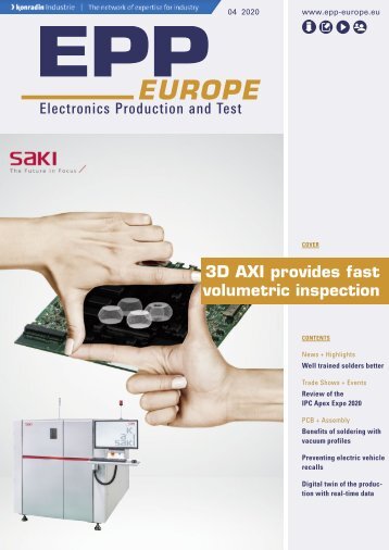
- Page 1 and 2: 04 2020 www.epp-europe.eu COVER 3D
- Page 3 and 4: EDITORIAL Fight against the virus S
- Page 5 and 6: Source: Saki Europe 38 Improving pe
- Page 7 and 8: EPP EUROPE April 2020 7
- Page 9 and 10: Techniques and parameters of the SM
- Page 11 and 12: Appointment of Director of EMEA Ope
- Page 13 and 14: Staff changes within sales partners
- Page 15 and 16: Source: EPP Europe / Doris Jetter 4
- Page 17 and 18: TRADE SHOWS + EVENTS Four inspectio
- Page 19 and 20: Koh Young Europe GmbH 0001754816-03
- Page 21 and 22: COVER 3D X-ray provides inspection
- Page 23 and 24: COVER Sliced image by tomosynthesis
- Page 25 and 26: COVER for the board to be loaded. M
- Page 27 and 28: PCB + ASSEMBLY The system has a fiv
- Page 29 and 30: PRODUCT UPDATES PCB + ASSEMBLY Smar
- Page 31: separate from the board. This can a
- Page 35 and 36: PCB + ASSEMBLY Design of a convecti
- Page 37 and 38: PRODUCT UPDATES PCB + ASSEMBLY Ther
- Page 39 and 40: PCB + ASSEMBLY Source: Electrolube
- Page 41 and 42: PCB + ASSEMBLY Sources 1) https://e
- Page 43 and 44: PCB + ASSEMBLY The traffic light co
- Page 45 and 46: PRODUCT UPDATES PCB + ASSEMBLY Auto
- Page 47 and 48: PCB + ASSEMBLY Optimizing material
- Page 49 and 50: PRODUCT UPDATES PCB + ASSEMBLY Comp
- Page 51 and 52: these manufacturers typically have
- Page 53 and 54: PRODUCT UPDATES PCB + ASSEMBLY Auto
- Page 55 and 56: PCB + ASSEMBLY Influence of thermal
- Page 57 and 58: PRODUCT UPDATES PCB + ASSEMBLY Deve
- Page 59 and 60: Technical cleaning solutions highli
- Page 61 and 62: Source: SMT Thermal Discoveries spa
- Page 63 and 64: Robotic process automation solution
- Page 65 and 66: AOI module with artificial intellig
- Page 67 and 68: Industrie The network of expertise
Inappropriate
Loading...
Mail this publication
Loading...
Embed
Loading...

