Electron Microscopy Solutions for NanoResearch - FEI Company
Electron Microscopy Solutions for NanoResearch - FEI Company
Electron Microscopy Solutions for NanoResearch - FEI Company

Create successful ePaper yourself
Turn your PDF publications into a flip-book with our unique Google optimized e-Paper software.
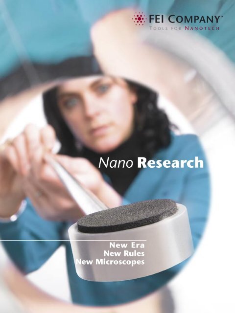
Nano Research<br />
New Era<br />
New Rules<br />
New Microscopes
R e s e a r c h<br />
Nanotechnology<br />
The next big thing<br />
Much that occurs in the macro-world of our<br />
everyday experience is ultimately determined<br />
by processes and phenomena that operate<br />
on the nanoscale - the scale of individual at-<br />
oms and molecules, and the <strong>for</strong>ces that act<br />
between them. This realization itself is not<br />
new. What is new is the growing collection of<br />
tools that allows us to explore and manipulate<br />
our world at this fundamental scale - Tools<br />
<strong>for</strong> Nanotech. This realization, these tools,<br />
and the creativity and ingenuity of individual<br />
researchers and their organizations together<br />
constitute the Nanotechnology Revolution -<br />
the next big thing.<br />
Nanotechnology has the potential to impact<br />
nearly every aspect of our daily lives. Practi-<br />
cal applications already exist, from stain-re-<br />
sistant fabrics to scratch-resistant automotive<br />
coatings, but these are only the beginning.<br />
Researchers are exploring new applications<br />
in chemistry, materials, space, energy, in<strong>for</strong>-<br />
mation, communication, transportation, and<br />
conservation. Some of these new applications<br />
will create new industries or radically change<br />
existing ones. New industries will create new<br />
economies, pose new dangers and ultimately<br />
reweave the very fabric of our societies.
Our future is driven by your challenges<br />
Nanotechnology is a broad term - some might say too broad<br />
- and its breadth creates a unique set of challenges <strong>for</strong> those<br />
who would work there. It is by nature multidisciplinary, and<br />
success requires collaboration across traditionally separate<br />
fields of knowledge. At <strong>FEI</strong> <strong>Company</strong> we embrace this col-<br />
laborative model at every level. It shapes our organization,<br />
directs our research, in<strong>for</strong>ms our new product development,<br />
designs our facilities, and directs our communications. One<br />
example is our network of “NanoPorts”, expressly designed<br />
to seek out opportunities to work with our customers to<br />
understand and solve their research problems. At the other<br />
end of the scale, in the design of hardware and software, we<br />
strive to incorporate networking, communication and data<br />
sharing capabilities at every level.<br />
At <strong>FEI</strong> we make the invisible visible - so that your work advances<br />
and your organization succeeds.<br />
We are <strong>FEI</strong> <strong>Company</strong><br />
At <strong>FEI</strong> we know that our success depends on yours, and you, in turn, rely on the quality and reliability of the tools we<br />
provide. The nano revolution is still young, and though its promise is widely recognized, so too are its risks. Successful<br />
execution on early opportunities can provide huge rewards, but such enterprises are fraught with uncertainties and there<br />
are plenty of competitors waiting to capitalize on mistakes. The selection of your most fundamental tools will be among<br />
the most important decisions you will make.<br />
Of course the tools you select must provide the best possible per<strong>for</strong>mance against the criteria you define today, but<br />
equally important they must have the flexibility and expandability to address the requirements you won’t discover until<br />
tomorrow. No system that you buy today can possibly accommodate all possible future needs. So, in choosing a system<br />
you are also choosing a partner, one that you will need to rely on <strong>for</strong> the life of the instrument, not only to support its<br />
current capabilities but also to develop new capabilities to address needs that are as yet unknown.<br />
Our desire to meet future needs does not reduce our commitment to current needs. Quality and reliability are built into<br />
our products at every level and our global service organization is second to none. We offer extensive training programs<br />
ENERGY<br />
EDUCATION<br />
DEMOCRACY<br />
DISEASE<br />
POPULATION<br />
Humanities<br />
challenges<br />
ENVIRONMENT<br />
TERRORISM<br />
& WAR<br />
POVERTY<br />
that range from basic operation and maintenance to advanced technique and collaborative methods development.<br />
WATER<br />
Dr. Richard Smalley, 1996 Chemistry Nobel prize winner, first started to relate<br />
nanotechnology with challenges facing humanity. The figure above names<br />
key problems and challenges of today’s society that could be improved or<br />
solved with the use of nanotechnologies.<br />
3
4<br />
Our heritage of<br />
technical leadership,<br />
our commitment to<br />
collaborative product<br />
development, and<br />
the demonstrably<br />
superior per<strong>for</strong>mance<br />
of our<br />
products combine<br />
to make <strong>FEI</strong> your<br />
best choice in<br />
Tools <strong>for</strong><br />
Nanotechnology.<br />
The image was taken by Robert Best <strong>for</strong><br />
Alasdair Wilson, both of the Advanced<br />
Materials Research Institute, UK.
We are <strong>FEI</strong> <strong>Company</strong><br />
We make Tools <strong>for</strong> Nanotech - scanning and transmission electron mi-<br />
croscopes (SEM and TEM) and focused ion beam (FIB) systems - that<br />
allow you to visualize, analyze and manipulate your world at the nano<br />
scale. We are a global technology company with more than 6 decades<br />
of leadership in imaging and analytical instrumentation. Throughout<br />
that time we have been pioneers in our chosen technologies, introduc-<br />
ing one of the first commercial TEMs in 1949, and the first DualBeam<br />
(FIB/SEM) system in 1993. Our new Titan S/TEM offers the best imaging<br />
resolution available today, 0.7 Ångström, sufficient to resolve individual<br />
atoms in many materials.<br />
We are determined to continue to lead our industry and we know that to<br />
do so we must nurture and maintain relationships with leading scientists<br />
and research organizations among our customers. The knowledge net-<br />
work that this approach creates is a resource that works both ways, pro-<br />
viding us with an awareness of current and future needs in the research<br />
marketplace, and our customers with access to knowledge and solutions<br />
across a broad range of applications. Together with our customers we<br />
strive to be thought-leaders, offering creative and innovative solutions<br />
that will drive the continuing development of nanotechnology.<br />
Continuous innovation<br />
Technology waits <strong>for</strong> no one. Our desire to play a leading role in the<br />
development of nanotechnology requires that we embrace a culture of<br />
continuous innovation. The leading edge of a revolutionary technology<br />
is not often a com<strong>for</strong>table place to be, but a willingness to accept risk<br />
is the ante to play in this high-stakes game. Breakthrough results are<br />
seldom discovered along a well trodden path.<br />
Our new Titan S/TEM, which offers unprecedented improvement in<br />
image resolution, is a case-in-point. Though the aberration correction<br />
technology that underlies the improvement is well known, <strong>FEI</strong> alone<br />
took the risk of incor<br />
porating it in a new TEM. As a result the Titan offers directly interpre-<br />
table image resolution 2 to 3 times better than uncorrected TEMs.<br />
As is often the case, innovation begets innovation. The incorporation of<br />
aberration correctors permits the design of larger lenses which in turn<br />
allows room <strong>for</strong> new technologies that maintain or control the sample<br />
environment. We can use this freedom to expand the types of samples<br />
and in situ procedures possible in an electron microscope. We want<br />
to relieve the researcher of the burden of adapting the sample to the<br />
microscope - instead, adapting the microscope to the sample.<br />
NanoPort<br />
<strong>FEI</strong>’s unique NanoPorts, located<br />
in the Netherlands, the United<br />
States, and Japan, are tangible<br />
evidence of our commitment to<br />
customer-centered collaboration.<br />
They provide a direct conduit<br />
<strong>for</strong> customer involvement in our<br />
development, engineering, training,<br />
testing and demonstration<br />
activities.<br />
Titan 80-300<br />
The Titan microscope incorporates<br />
a newly designed plat<strong>for</strong>m<br />
dedicated to the principles of<br />
ultimate stability, ultimate per<strong>for</strong>mance<br />
and ultimate flexibility<br />
<strong>for</strong> corrector and monochromator<br />
technology and its applications.<br />
5
6<br />
With <strong>FEI</strong>’s tools <strong>for</strong><br />
<strong>NanoResearch</strong><br />
<strong>FEI</strong> offers a range of Tools <strong>for</strong><br />
Nanotech, each with particular strengths<br />
in a range of applications. <strong>NanoResearch</strong><br />
applications may be roughly grouped<br />
into 5 categories: material qualifi cation,<br />
material and tool preparation, prototyping,<br />
metrology, and device testing and<br />
characterization<br />
• SEMs like the Quanta FEG can<br />
visualize surface topography with<br />
a resolution of 1 - 2 nm resolution<br />
• The Nova NanoSEM improves on<br />
the resolution of the Quanta by using<br />
an “immersion” type objective lens<br />
• Nova NanoLab combines high<br />
resolution SEM imaging with a FIB<br />
<strong>for</strong> cutting sample cross sections that<br />
reveal subsurface features<br />
• Helios NanoLab is the next<br />
generation DualBeam, providing<br />
resolution to the sub-nanometer level,<br />
producing the thinnest samples of the<br />
highest quality<br />
• Tecnai TEMs are research grade<br />
instruments that offer sub-Ångström<br />
in<strong>for</strong>mation limits in a wide variety of<br />
lens confi gurations<br />
• The Titan S/TEM offers aberration<br />
correctors <strong>for</strong> directly interpretable,<br />
sub-Ångström image resolution.<br />
Quanta FEG<br />
Nova NanoSEM<br />
Nova NanoLab<br />
Helios NanoLab<br />
Tecnai TEM<br />
Titan 80-300<br />
SEM/ESEM<br />
SEM-FIB<br />
TEM/STEM<br />
Materials & Device<br />
Characterization<br />
���<br />
���<br />
���<br />
��<br />
�<br />
�<br />
����<br />
����<br />
����<br />
����<br />
����<br />
����<br />
����<br />
����<br />
GaAs<br />
GaAIAs<br />
�<br />
�<br />
����<br />
����<br />
����<br />
����<br />
����<br />
����<br />
����<br />
����<br />
�� �� �� �� ��<br />
��<br />
GaAIAs<br />
GaAs<br />
�<br />
� ��� ��� ��� ��� ��� ��� ��� ��� ���<br />
���<br />
���<br />
���<br />
��<br />
GaAs<br />
GaAIAs<br />
�� �� �� �� ��<br />
��<br />
GaAIAs<br />
GaAs<br />
�<br />
� ��� ��� ��� ��� ��� ��� ��� ��� ���
Sample Preparation<br />
and Manipulation<br />
Nano<br />
Metrology<br />
courtesy:<br />
Weizmann Institute<br />
Nano Preparation<br />
and Fabrication<br />
7
<strong>NanoResearch</strong> requirements<br />
The rapid pace of innovation in nanotechnology places<br />
a premium on certain aspects of overall system design.<br />
These concepts receive high priority in <strong>FEI</strong> tools:<br />
8<br />
• Capability<br />
meet the immediate needs of existing<br />
or anticipated projects<br />
• Flexibility<br />
adapt to a broad range of requirements<br />
without additional hardware/software<br />
• Modularity<br />
add capability as required without replacing<br />
the base system, thus preserving the long-term<br />
value of the initial investment<br />
• Productivity<br />
generate more value faster.<br />
• Connectivity<br />
enhance communication within the<br />
system, across the lab or around the world<br />
• Compatibility<br />
extend the range of samples and<br />
experimental conditions
10<br />
Key capabilities<br />
• Visualize<br />
The primary requirement <strong>for</strong> any microscope is certainly<br />
resolution. TEM manufacturers talk about two kinds of<br />
resolution: image resolution (or point resolution) that<br />
can be directly interpreted from an image, and the<br />
in<strong>for</strong>mation limit, the finest detail that can be trans-<br />
ferred by the optical system, though not directly observ-<br />
able because of lens aberrations. Aberration correctors<br />
bring image resolution down to the in<strong>for</strong>mation limit,<br />
making the full resolving power of the microscope<br />
directly observable in the images it produces.<br />
• Analyze<br />
Analytical resolution is often as important as imaging<br />
resolution. Analytical resolution (<strong>for</strong> energy loss spec-<br />
A heritage of innovation<br />
• DualBeam<br />
<strong>FEI</strong> invented the DualBeam, in which an SEM column<br />
is positioned to image the face of a cross section milled<br />
by a focused ion beam. Cross sections reveal subsurface<br />
structure and with automated “slice and view” routines<br />
can recreate three dimensional models from sequential<br />
slices.<br />
• ESEM<br />
<strong>FEI</strong> pioneered the ESEM (Environmental SEM) which<br />
permits direct observation of wet, contaminating, non-<br />
conductive samples.<br />
• Aberration correctors<br />
The Titan is the first TEM to be designed specifically<br />
<strong>for</strong> spherical aberration correctors, breaking once and<br />
<strong>for</strong> all the 1 Ångström barrier <strong>for</strong> directly interpretable<br />
image resolution..<br />
• Monochromator<br />
The Titan also incorporates monochromator technology<br />
to reduce chromatic aberrations and improve the energy<br />
resolution of electron energy loss spectrometry (EELS).<br />
troscopy) depends on the energy distribution of the<br />
beam and the spectrometer’s ability to resolve the<br />
energy of transmitted electrons.<br />
• Manipulate and control<br />
Ultimately we want to manipulate the sample on the<br />
nano-scale in an environment of our choosing. Ion<br />
beams can remove or deposit material with nano-scale<br />
precision. Specialized vacuum and detector technologies<br />
permit the use of non-high-vacuum environments that<br />
accommodate a wider range of samples and permit<br />
observations of samples in a natural or controlled<br />
experimental environment, and allow the introduction<br />
of selected gases that work with the electron or ion<br />
beam to modify the sample.<br />
• Tomography<br />
Automatically acquired rotational sequences of 2D<br />
TEM projections are mathematically combined into 3D<br />
models.<br />
• Gas chemistry<br />
Designer gases introduced into the ion or electron beam<br />
path can selectively accelerate material removal or<br />
deposition to create structure with nano-scale control.<br />
• Automation<br />
Automated setup, data acquisition, image processing,<br />
3D modeling, and compositional analysis vastly improve<br />
productivity and reliability, and reduce requirements <strong>for</strong><br />
operator training and expertise.
<strong>FEI</strong> <strong>Company</strong><br />
World Headquarters and<br />
North American Sales<br />
5350 NE Dawson Creek Drive<br />
Hillsboro, OR 97124-5793 USA<br />
Tel: +1 503 726 7500<br />
Fax: +1 503 726 7509<br />
European Sales<br />
Tel: +31 40 23 56 110<br />
Fax: +31 40 23 56 612<br />
Asia-Pacific Sales<br />
Tel: +65 6272 0050<br />
Fax: +65 6272 0034<br />
Japan Sales<br />
Tel: +81-3-3740-0970<br />
Fax: +81-3-3740-0975<br />
e-mail: sales@fei.com<br />
www.fei.com<br />
04MB_OT0111 08_06<br />
©2006. We are constantly improving the per<strong>for</strong>mance of our products,<br />
so all specifications are subject to change without notice. The <strong>FEI</strong> logo,<br />
Tools <strong>for</strong> Nanotech, Quanta, Nova, Helios NanoLab, Tecnai, and Titan,<br />
are trademarks of <strong>FEI</strong> <strong>Company</strong>. Windows is a trademark of Microsoft<br />
Corporation.