PECVD: The Linear Cluster Tool â Phoebus © â - Leybold Optics GmbH
PECVD: The Linear Cluster Tool â Phoebus © â - Leybold Optics GmbH
PECVD: The Linear Cluster Tool â Phoebus © â - Leybold Optics GmbH

Create successful ePaper yourself
Turn your PDF publications into a flip-book with our unique Google optimized e-Paper software.
A-Si/µc-Si Deposition Equipment<br />
Michael Liehr<br />
Photon‘s 5 th PV Production Equipment Conference<br />
(Thin Film), Stuttgart, April 2010
At a Glance<br />
<strong>Optics</strong><br />
Architectural<br />
Glas<br />
27/04/10<br />
-Markets- -Technology- -Locations-<br />
Photovoltaics<br />
Automotive<br />
Electronics/<br />
packaging<br />
design and production<br />
of equipment and processes<br />
for vacuum coating<br />
Over 1.000 systems built<br />
Currently ~500 employees w/w<br />
M Liehr, Photon‘s 5th PV Production Equipment Conference, Stuttgart, 2010<br />
Alzenau / Germany<br />
Sales, service, production and R & D<br />
Dresden / Germany<br />
Sales, service, production and R & D<br />
Cary, USA<br />
Sales, service and production<br />
Beijing, China<br />
Sales, service, production and R & D<br />
1
<strong>The</strong> Silicon Thin Film Solar Cell<br />
Options:<br />
Front contakt (PVD):<br />
• SnO 2 :F<br />
• ZnO:B<br />
• ZnO:Al<br />
• ZnO:Ga<br />
Absorber (<strong>PECVD</strong>):<br />
• 13,56 MHz <strong>PECVD</strong><br />
• VHF <strong>PECVD</strong><br />
Back contakt (PVD):<br />
• ZnO:Al + Ag + Al<br />
• ZnO:Ga + Ag + Ti<br />
• ZnO:B + white colour<br />
PVD = Physical Vapour<br />
Deposition<br />
<strong>PECVD</strong> = Plasma Enhanced<br />
Chemical Vapour Deposition<br />
Transparent<br />
Electrode<br />
(PVD)<br />
Back<br />
Electrode<br />
(PVD)<br />
p<br />
i<br />
n<br />
p<br />
i<br />
n<br />
Glass<br />
(SiO2)<br />
TCO ZnO:Al / SnO:F<br />
a-Si:H (~300 nm)<br />
µc-Si:H µc-Si:H (~1300 nm)<br />
TCO ZnO:Al<br />
Ag<br />
Al<br />
Every interface<br />
is micro rough<br />
Top Cell<br />
(<strong>PECVD</strong>)<br />
Bottom Cell<br />
(<strong>PECVD</strong>)<br />
M Liehr, Photon‘s 5th PV Production Equipment Conference, Stuttgart, 2010 2
<strong>The</strong> a-Si/µc-Si Production Line<br />
�Typical factory layout:<br />
< 70 sec tact<br />
~60 MWp/a @ 8.5% eff.<br />
Gen 5 Glas (1.4x1.1 m 2 )<br />
� Glass transport in<br />
closed conveyors under<br />
cleanroom conditions<br />
�Factory layout can be<br />
tailored to local requirements<br />
PVD = Physical Vapour<br />
Deposition<br />
<strong>PECVD</strong> = Plasma Enhanced<br />
Chemical Vapour Deposition<br />
60 Megawatts annual production unit<br />
P2<br />
6 x <strong>PECVD</strong> (absorber)<br />
PVD (back contact)<br />
ca. 150 metres<br />
P1<br />
P3<br />
PVD TCO (front contact)<br />
M Liehr, Photon‘s 5th PV Production Equipment Conference, Stuttgart, 2010<br />
Back end<br />
<strong>Leybold</strong> <strong>Optics</strong>‘ core competences are<br />
vacuum systems and processes:<br />
<strong>PECVD</strong> (light absorber) and PVD (electrode/transparent electrode)<br />
3
PVD: Magnetron Sputter Systems<br />
�Designed for sputtering<br />
of transparent conductive<br />
oxides (TCO) and metals<br />
for front and back<br />
contacts of thin film<br />
solar cells from metallic<br />
or ceramic targets<br />
�Made from stainless<br />
steel (or carbon steel on<br />
demand)<br />
� Production proven<br />
� Horizontal and vertical<br />
�With and without carrier<br />
� Ambient temperature<br />
or heated<br />
A 1500 V-7<br />
Cylindrical magnetron sputter cathode<br />
(with plasma racetrack)<br />
M Liehr, Photon‘s 5th PV Production Equipment Conference, Stuttgart, 2010 4
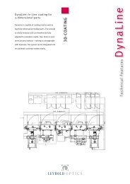
<strong>PECVD</strong>: <strong>The</strong> <strong>Linear</strong> <strong>Cluster</strong> <strong>Tool</strong> „ <strong>Phoebus</strong> © “<br />
�System consisting of<br />
vacuum tunnel with robot,<br />
loadlock chambers and<br />
14 <strong>PECVD</strong> process<br />
chambers<br />
� Single process<br />
chambers can be removed<br />
during system<br />
operation<br />
� All process chambers<br />
fitted with oil heating<br />
� Process chambers<br />
cleaned with NF 3<br />
remote plasma<br />
M Liehr, Photon‘s 5th PV Production Equipment Conference, Stuttgart, 2010 5
<strong>PECVD</strong>: <strong>The</strong> <strong>Linear</strong> <strong>Cluster</strong> <strong>Tool</strong> „ <strong>Phoebus</strong> © “<br />
� Gen 5 substrates<br />
(1.4x1.1 m 2 )<br />
� Substrate temperature<br />
maintained during transport<br />
�Rigorous gas separation<br />
� High flexibility in process<br />
sequence<br />
� New process steps can<br />
be implemented easily<br />
� Vertical but carrier free<br />
concept<br />
� No break of vacuum<br />
during PIN-PIN process<br />
� High redundancy<br />
� Integrated failure<br />
management<br />
� Rectangular shape fits<br />
easily in most production<br />
facilities<br />
L - substrate loading,<br />
heating<br />
U - substrate<br />
unloading,cooling<br />
V - gate valves<br />
Sh - shuttle – handling<br />
robot with sustaining<br />
heater<br />
R - rails for shuttle<br />
P - process chamber<br />
dP - detached process<br />
chamber<br />
dP<br />
U<br />
P<br />
Sh<br />
M Liehr, Photon‘s 5th PV Production Equipment Conference, Stuttgart, 2010 6<br />
L<br />
V<br />
R<br />
T
<strong>PECVD</strong>: <strong>The</strong> <strong>Linear</strong> <strong>Cluster</strong> <strong>Tool</strong> „ <strong>Phoebus</strong> © “<br />
<strong>The</strong> handling robot inside<br />
the vacuum tunnel<br />
� 5°tilted (vs. vertical)<br />
handling robot with<br />
stations for 2 glass<br />
sheets (in/out), no carriers<br />
� v max = 0.8 m/sec,<br />
dv/dt = 1.8 m/sec²<br />
� Both stations heated<br />
to maintain temperature,<br />
power/cooling water by<br />
„supply chain“<br />
� Powered by linear<br />
drive motors<br />
Gate valves to process chambers<br />
Handling<br />
robot<br />
Drag chain<br />
for media supply<br />
M Liehr, Photon‘s 5th PV Production Equipment Conference, Stuttgart, 2010 7
<strong>PECVD</strong>: <strong>The</strong> <strong>Linear</strong> <strong>Cluster</strong> <strong>Tool</strong> „ <strong>Phoebus</strong> © “<br />
<strong>The</strong> plasma reactor:<br />
� <strong>PECVD</strong> process chamber<br />
with 13,56 MHz<br />
parallel plate configuration<br />
and integrated<br />
showerhead for gas supply<br />
�Small gap between<br />
life electrode and substrate<br />
(10-15 mm) and<br />
high process gas<br />
pressure (several mbar)<br />
(IPV FZ Jülich Process)<br />
�Absolute control over<br />
reactor temperature which<br />
is extremely important<br />
for avoiding dust<br />
formation<br />
M Liehr, Photon‘s 5th PV Production Equipment Conference, Stuttgart, 2010<br />
Counter electrode<br />
with substrate pick-up<br />
Life electrode with<br />
gas shower head<br />
8
<strong>PECVD</strong>: <strong>The</strong> <strong>Linear</strong> <strong>Cluster</strong> <strong>Tool</strong> „ <strong>Phoebus</strong> © “<br />
Gen 5 a-Si single<br />
junction solar cell:<br />
� max/min deviation<br />
from average cell<br />
thickness: 4,7%<br />
� Sigma: < 2,0%<br />
Gen 5 µc-Si single<br />
junction solar cell:<br />
�max/min deviation<br />
from average cell<br />
thickness: 6,4%<br />
� Sigma: < 2,3%<br />
M Liehr, Photon‘s 5th PV Production Equipment Conference, Stuttgart, 2010 9
<strong>PECVD</strong>: <strong>The</strong> <strong>Linear</strong> <strong>Cluster</strong> <strong>Tool</strong> „ <strong>Phoebus</strong> © “<br />
µc-Si solar cells<br />
� Crystallinity of silicon<br />
very susceptible to<br />
silane dilution in<br />
hydrogen plasma AND<br />
underlying surface<br />
� Transition region<br />
between microcrystalline<br />
silicon and amorphous<br />
silicon provides<br />
highest cell efficiency<br />
(region marked in<br />
yellow/dotted line)<br />
� Excellent process<br />
control necessary<br />
across entire<br />
subtrate area<br />
Kristallinität [%].<br />
90<br />
80<br />
70<br />
60<br />
50<br />
40<br />
30<br />
20<br />
10<br />
0<br />
Crystallinity vs. Silane dilution<br />
on glass<br />
on TCO<br />
-10<br />
0,35%0,45%0,55%0,65%0,75%0,85%0,95%1,05%1,15%1,25%1,35%1,45%1,55%1,65%<br />
Silane dilution<br />
Silane dilution<br />
M Liehr, Photon‘s 5th PV Production Equipment Conference, Stuttgart, 2010 10
<strong>PECVD</strong>: <strong>The</strong> <strong>Linear</strong> <strong>Cluster</strong> <strong>Tool</strong> „ <strong>Phoebus</strong> © “<br />
� µc-Si solar cell:<br />
crystallinity across<br />
the entire subtrate<br />
area (Gen 5)<br />
measured by<br />
Raman probe<br />
(ratio [abs(%)]<br />
Sigma: 1,73%<br />
cm<br />
M Liehr, Photon‘s 5th PV Production Equipment Conference, Stuttgart, 2010<br />
cm<br />
11
<strong>The</strong> <strong>Leybold</strong> <strong>Optics</strong> a-Si/µc-Si Module<br />
Production status:<br />
� Front contact:<br />
(SnO:F)<br />
� I-Layer of bottom<br />
cell 1,35 µm<br />
� Results before<br />
light soaking and<br />
and lamination:<br />
Rs = 11,8 Ω<br />
FF = 71%<br />
Uoc = 145 V<br />
Isc = 1,4 A<br />
η = 9,9 % (best)<br />
η = 9,4 % (average)<br />
Champion cells<br />
from lab line:<br />
η ~ 11 %<br />
(initial)<br />
Module Generation 5 (1,4 x 1,1 m 2 cell size)<br />
M Liehr, Photon‘s 5th PV Production Equipment Conference, Stuttgart, 2010<br />
12
Production Output<br />
Production data<br />
� Cell efficiency<br />
before light soaking<br />
Module efficiency Feb-Apr 2010<br />
Lessons learned:<br />
• Well defined interfaces between different suppliers of line equipment<br />
absolutely necessary<br />
• Glass quality/TCO glass quality crucial for cell performance<br />
• Vertical linear cluster tool PHOEBUS now production proven<br />
M Liehr, Photon‘s 5th PV Production Equipment Conference, Stuttgart, 2010<br />
13
Challenges for Thin Film Si Solar Cells<br />
We now see two<br />
main challenges for<br />
thin film silicon solar<br />
cells:<br />
�Module efficiency<br />
is most important<br />
because of over-supply<br />
� Cost/price per Wp is<br />
the second challenge<br />
since reaching high<br />
module efficiencies<br />
still needs to be<br />
profitable<br />
1. Module Efficiency<br />
- Module efficiency over 10% stabilized already a „must“.<br />
This is a challenge for thin film silicon<br />
→ many smaller iterative steps<br />
2. Cost/Price per Wp<br />
- Price for p-Si dropped from 480 US$/kg (2008)<br />
to 60 US$/kg (2009/10)<br />
- AMAT modules at 1.30-1.50 US$/Wp<br />
vs. First Solar
Challenges for Thin Film Si Solar Cells<br />
� Improving cell/module<br />
efficiency is the sum of<br />
many smaller measures<br />
� Improving productivity<br />
is achieved by fewer but<br />
more significant steps<br />
Improvement of Productivity (+cell efficiency)<br />
• Change to Ar/F2 for in-situ cleaning of reactors [in progress]<br />
• Replace RF (13.56 MHz) by VHF [future]<br />
• Extend RF to Dual Frequency (13.56/27.12 MHz) [in progress]<br />
Influence of bias voltage on crystallinity/efficiency of Si TF cells<br />
Source: Amanatides 2001<br />
J.Appl.Phys., Vol 90, No11<br />
M Liehr, Photon‘s 5th PV Production Equipment Conference, Stuttgart, 2010<br />
Source:<br />
Deng, 2006<br />
NREL Subcontract<br />
ZXL-5-44205-06<br />
15
<strong>PECVD</strong>: Dual Frequency – New Concept<br />
Problem: cell efficiency<br />
deteriorates with higher<br />
<strong>PECVD</strong> deposition rates<br />
<strong>The</strong>refore:<br />
DUAL FREQUENCY<br />
� Control of bias voltage<br />
is extremely important for<br />
the deposition of µc<br />
material<br />
�Bis voltage can be switched<br />
from positive to negative<br />
values by simply changing<br />
the phase shift on a<br />
frequency generator<br />
�Patented by University<br />
of Bochum, Germany, and<br />
exclusively licenced<br />
to <strong>Leybold</strong> <strong>Optics</strong> for PV<br />
UDc>0<br />
UDc
<strong>PECVD</strong>: Dual Frequency – New Concept<br />
DUAL FREQUENCY<br />
� Higher efficiencies<br />
at high deposition<br />
rates (2*times higher)<br />
�Even better uniformity<br />
than 13.56 MHz<br />
alone<br />
relative efficiency<br />
105%<br />
100%<br />
95%<br />
90%<br />
85%<br />
80%<br />
75%<br />
70%<br />
65%<br />
60%<br />
55%<br />
50%<br />
Comparison RF (13 MHz) with DF-Technique<br />
a-Si junction (300nm)<br />
0,00 0,10 0,20 0,30 0,40 0,50 0,60 0,70 0,80 0,90 1,00<br />
deposition rate [nm/s]<br />
50 150 250 350 450 550 650 750 850 950 1050<br />
50 473 478 481 482 482 483 484 481 480 476 471<br />
150 473 483 487 488 496 497 498 496 493 485 478<br />
250 482 495 501 503 503 507 510 513 512 500 484<br />
350 486 502 507 509 510 517 521 521 520 508 487<br />
450 491 507 512 514 517 518 522 523 523 513 493<br />
550 493 506 510 513 516 523 524 524 524 513 494<br />
650 491 503 508 511 513 523 524 524 524 515 496<br />
750 489 500 503 504 509 521 525 524 524 518 496<br />
850 490 498 500 498 505 519 523 523 524 518 496<br />
950 489 494 496 494 493 510 515 518 521 512 494<br />
1050 487 489 492 491 492 505 511 513 517 508 497<br />
1150 485 487 488 488 491 497 505 509 510 503 494<br />
1250 480 489 488 487 493 496 499 503 504 496 483<br />
1350 476 482 487 491 500 504 504 501 498 484 479<br />
DF Technique<br />
RF 13 Mhz Technique<br />
1 2 3 4 5 6 7 8 9 10 11<br />
50 150 250 350 450 550 650 750 850 950 1050<br />
50 651 649 634 632 626 641 658 674 667 646 628<br />
150 644 657 666 666 657 633 627 627 636 642 643<br />
250 653 675 679 668 660 650 637 627 631 628 634<br />
350 630 659 658 640 646 648 640 627 637 646 648<br />
450 651 641 631 649 667 674 657 639 648 652 631<br />
550 652 636 636 664 669 662 654 640 635 634 626<br />
650 651 628 647 662 672 671 671 654 633 637 626<br />
750 645 628 656 655 653 662 664 642 635 648 626<br />
850 644 630 659 651 639 651 647 626 629 637 635<br />
950 626 641 683 668 640 655 643 628 627 636 650<br />
1050 647 670 688 669 650 660 633 630 641 634 651<br />
1150 661 686 678 659 652 649 631 634 645 647 646<br />
1250 657 668 664 675 659 643 644 654 674 644 641<br />
1350 663 683 699 659 641 654 675 666 661 655 645<br />
13.56 MHz 13.56MHz + 27.12 MHz<br />
2,8% Standard deviation 2,4 %<br />
M Liehr, Photon‘s 5th PV Production Equipment Conference, Stuttgart, 2010<br />
17
<strong>The</strong> End<br />
Thank you for your attention<br />
Further information at<br />
www.leyboldoptics.com<br />
M Liehr, Photon‘s 5th PV Production Equipment Conference, Stuttgart, 2010 18