

Build a Class-A Amplifier - Pass DIY
Build a Class-A Amplifier - Pass DIY
Build a Class-A Amplifier - Pass DIY

You also want an ePaper? Increase the reach of your titles
YUMPU automatically turns print PDFs into web optimized ePapers that Google loves.
<strong>Build</strong> a <strong>Class</strong>-A <strong>Amplifier</strong><br />
Audio Feb, 1977 by Nelson <strong>Pass</strong><br />
In spite of their high cost and low efficiency, class A power amplifiers have recently been<br />
receiving more attention from audiophiles who demand uncompromising accuracy. Both<br />
the price and quality of these amplifiers result from the operation of their output stages in<br />
class A mode, where the amplifying devices are constantly operated in their linear region,<br />
above cutoff and below saturation. Whether made from tubes or semiconductors, circuits<br />
operating in class A mode yield the smoothest transfer functions and widest bandwidths,<br />
hence their near universal application in preamplifiers and other low power circuitry.<br />
Most audio power amplifiers use class A circuitry except<br />
in the drive and output stages, where they use class B or<br />
AB operating modes to achieve high efficiency. In class<br />
B and AB modes, the output stage operates in a pushpull<br />
configuration, where one set of output devices<br />
delivers positive voltage and current and another set<br />
delivers negative voltage and current. When one set is<br />
working, the other set is turned off. This scheme<br />
operates efficiently, but has two serious flaws, the<br />
extremely nonlinear characteristic of the transistors at<br />
the collector cutoff region and the turn-on/turn-off times of the devices. Designers of<br />
transistor amplifiers have tended to use large amounts of negative feedback to correct for<br />
the nonlinearities, but this works well only at low frequencies. At high frequencies, the<br />
feedback loop is unable to make adequate corrections, and the distortion that occurs at the<br />
output is aggravated by overloaded front-end circuitry.<br />
The usual total harmonic and intermodulation<br />
distortion figures do not reveal the abrupt output stage<br />
distortions accurately because of the averaging factor<br />
involved in such measurements. A spike of crossover<br />
distortion may reach 2 per cent, but if it occurs only<br />
over 5 per cent of the waveform, it averages out to a<br />
respectable 0.1 per cent distortion figure. Considering<br />
this error factor, it is easy to see why two amplifiers<br />
with the same specifications can sound so different. To<br />
properly evaluate the distortion, peak distortion and<br />
harmonic distribution must be considered. Typical class A amplifiers will exhibit low<br />
order harmonics, and their peak distortion is less than twice the average distortion. In<br />
class AB amplifiers, very high orders of harmonics occur, and the peak distortion can be<br />
as much as thirty times the average distortion.<br />
Another problem common to class B and AB output stages is due to the unequal turnon/turn-off<br />
times of the transistors. Because the turn-off time is greater, both transistor
sets can conduct uncontrollably under high slew conditions, making it dangerous to<br />
operate the amplifier at high frequencies, a particularly bad problem with some quasicomplementary<br />
designs.<br />
In a class A output stage, however, there are no abrupt nonlinearities and no turn-on/turnoff<br />
delays. The smooth transfer characteristic yields low order harmonic distortions, and<br />
these harmonics can easily become unmeasurable at low power levels.<br />
Circuitry<br />
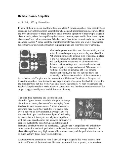
In the course of our research, we developed a small class A power amplifier which<br />
delivers 20 watts into 8 ohms. It offers excellent performance over a wide bandwidth, and<br />
the design is simple and stable enough that it can be built by the advanced constructor at<br />
low cost and with a minimum of test equipment. The parts utilized are usually available<br />
off the shelf from Motorola and RCA distributors, and the design will accommodate the<br />
usual variations in components without problems, so that it is unnecessary to select<br />
semiconductors for particular characteristics. A stereo version of this amplifier can be<br />
built for approximately $200.00.<br />
The basic circuit configuration is shown in Fig. 1, where an input differential transistor<br />
pair drives a current-sourced transistor, forming the two voltage-gain stages of the<br />
amplifier. The output of the second voltage-gain transistor drives a triple emitter-follower<br />
output stage, which provides a current gain of somewhat less than a million. The four<br />
current sources in the circuit are used to simultaneously increase the bandwidth and<br />
linearity, accomplishing this by idling semiconductors at currents much larger than the<br />
currents required to drive the amplifier. With the exception of the output stage, the gain<br />
transistors operate with only small variations about their operating points.
The compensation capacitor shown in Fig. 1 is used to provide damping for the circuit,<br />
eliminating overshoot and ringing in the output. Its effect is the reverse of the usual lag<br />
compensation employed in transistor amplifiers because it actually reduces transient<br />
intermodulation effects by creating an internal high frequency feedback loop similar to<br />
the damping circuits found in servo systems, where the front end of the amplifier can<br />
satisfy its own loop requirements at high frequencies, avoiding front-end overload.<br />
The schematic of the actual amplifier is presented in Fig. 2. The transistors<br />
Q3,6,7,13,14,15,16 form the current sources of Fig. 1. Their current value is governed by<br />
the active voltage source of Q8, where the circuit is stabilized by taking feedback from<br />
R22. This current sourcing system accurately tracks the current value once it is properly<br />
adjusted. The one-toone circuit board pattern and an upsized parts location guide are<br />
given in Fig. 3 and Fig. 4. The location of the parts is self explanatory, except that Q5 and<br />
Q7 must be fitted with heat sinks. Reasonable care must be taken to avoid overheating the<br />
semiconductors and other components during soldering, and high-wattage soldering guns<br />
must not be used. If any substitute transistors are used, it may be necessary to adjust the<br />
values of C7 and C4 for stable operation using an 8-ohm non-inductive load and driving<br />
the amplifier with 100 kHz square waves. If the amplifier should exhibit high frequency<br />
oscillation, increase the value of C4 or decrease the value of C7.
For this amplifier, there is no such thing as too much heat sinking for the output stage.<br />
Extravagance in this area is no vice, and good ventilation is similarly very important. The<br />
use of more than 100 square inches of black-anodized aluminum heat sink per output<br />
transistor should allow for operation without a fan. A safe rule of thumb by which to<br />
evaluate the quality of heat sinking is to see whether or not you can place your hand on<br />
the heat sink without hurting yourself. The heat sink should be grounded to the chassis of<br />
the amplifier, and heat-conducting insulators must be used with a liberal quantity of<br />
silicone grease between the heat sink and the output transistors.
Figure 5 shows the power supply for a two-channel system which will allow different<br />
supply voltages for optimization of the output power versus load impedance. The 105<br />
volt primary tap of the transformer will serve for 8-ohm loads, the 115 volt tap for 6-ohm<br />
loads, and the 125 volt tap for 4-ohm loads. With a 120 volt a.c. line, the maximum<br />
power yield is 20 watts per channel into 8 ohms, 24 watts into 6 ohms, and 28 watts into<br />
4 ohms. To alter the amplifier for optimal performance into a given load, the tap must be<br />
changed and the amplifier must be rebiased. If the diode bridges in the power supply are<br />
not mounted on a metal chassis, they too must be provided with heat sinks. Use 16-gauge<br />
wiring in the power supply and amplifier output connections, while 24-gauge wire is<br />
adequate for other connections. It is important that all of the ground connections be<br />
shared by both channels at one point on the ground bus. The ground bus must connect all<br />
four power supply capacitors and be of heavy gauge. Additional wiring information is<br />
given in Fig. 6, where the grounding and power connections are to be followed literally<br />
for low noise. At the input connectors, the ground of the input is physically isolated from<br />
the chassis. A 0.1 uF capacitor connects each input ground to the chassis at the input and<br />
is used to eliminate r.f. pickup.
Set Up<br />
Biasing the amplifier is quite easy with either a d.c. voltmeter or an oscilloscope. Before<br />
turning on the amplifier, R16 must be adjusted for maximurn resistance (minimum bias<br />
current). If the bias is set too high, the negative power supply fuse will blow without<br />
damaging the circuit. If this occurs at one extreme setting of the potentiometer, replace<br />
the fuse, set the pot to the other extreme, and try again. After the amplifier is turned on<br />
and doesn't blow the fuses, the bias must be set by adjusting R16, preferably using an<br />
oscilloscope. Using an oscilloscope, the bias is adjusted by driving the amplifier with a<br />
sine wave into the appropriate load resistor value. Set R16 so that the amplifier clips into<br />
the load on the negative half of the wave before the positive half clips. Then operate the<br />
amplifier for 15 minutes without an input signal. After 15 minutes, readjust the bias for<br />
symmetrical clipping of the circuit when it is very slightly overdriven. Repeat the<br />
adjustment again in 15 minutes to insure that the heat sinks have reached thermal<br />
equilibrium.<br />
If using a high quality d.c. voltmeter, the bias can be adjusted by a similar procedure,<br />
measuring the voltage occuring across R22. For an 8-ohm load, the voltage across R22<br />
should be 125 millivolts. For 6 ohms, the voltage is to be 170 mV, and 220 mV for 4ohm<br />
loads. As before, the bias must be adjusted slightly low and increased slowly to the<br />
proper value after the amplifier has warmed up. The voltage should be monitored and<br />
adjusted periodically over a half an hour or so.<br />
The prototype amplifier was built without specially selected components and the only<br />
adjustments made were the output bias currents. The amplifier yielded the performance<br />
figures shown in Table I.<br />
The amplifier's response to square waves is shown at 20 Hertz (Fig. 7) and at 100,000<br />
Hertz (Fig. 8). Figure 9 shows the waveform at 500,000 Hertz at —6 dB power level. All<br />
tests were conducted with non-inductive load resistors, but the performance remains<br />
unaltered with reactive elements in the load. The amplifier's distortion characteristics
emain virtually unchanged with fully reactive loads, and we were unable to detect a<br />
significant difference in harmonic amplitudes between an 8-ohm load and a 2-microfarad<br />
capacitor driven at 10 kiloHertz.<br />
The amplifier cannot be damaged by shorting the output or by overdriving the input. It<br />
does not require a load for stability and can be safely driven into any load at any<br />
frequency. The components are chosen for very conservative operation; for example, the<br />
output transistors are operated at a third their rated voltage, a tenth their rated continuous<br />
current, and about a tenth their dissipation capability, insuring a long life span for the<br />
amplifier.<br />
After extensive listening tests, we concluded that the sonic purity of the amplifier more<br />
than justifies its high power consumption (less than a color TV). The sound is neutral,<br />
and we have found it useful as a tool in evaluating preamplifier circuits, as it outperforms<br />
quite a few of them. It also serves well in driving electrostatic headphones and as the high<br />
frequency driver in a multi-amp system.<br />
Designer's Specifications<br />
Table 1<br />
Power: 20 watts/ch. 8 ohm, 24 watts/ch. 6 ohm, and 28 watts/ch. 4 ohm.<br />
Freq. Response: -3 dB at 0.33 Hertz, -3 dB at 500,000 Hertz.<br />
Slew Rate: 30 volts/microsecond, leading and trailing edges<br />
Damping Factor: 100 from d.c. to 50,000 Hertz.<br />
Noise: 0.8 millivolt at the output, primarily 120 Hertz.<br />
Harmonic Distortion: Below clipping, harmonics are limited to second and third; all other<br />
harmonics were below our 90-dB test residual; at 16 watts, 20,000 Hertz and 8 ohms, -73<br />
dB second, -74 dB third; at 10 watts, 20,000 Hertz and 8 ohms, -75 dB second, -75 dB<br />
third; at 5 watts, 20,000 Hertz and 8 ohms, -76 dB second; at lower frequencies and<br />
power levels, the distortion becomes very difficult to measure accurately.
Table 2 - Parts list for One Channel,<br />
Q1,2,3,8 Motorola MPSL01<br />
Q4 RCA 1A16<br />
Q5,6,7 RCA 1A15<br />
Q9-16 Motorola 2N5877<br />
D1,2 1N914<br />
D3 Any germanium diode<br />
D4,5 1N4004<br />
C1,2 1000 uF, PC mount electrolytic, 16 volt<br />
C3,4 75 pF, 5% polystrene, mica, or mylar<br />
C5,6 100 uF, 50V PC mount, electrolytic<br />
C7 0.004uF, 5%<br />
C8 0.1uF, 20%, 100V<br />
R1 1megohm, 5%, 1/4W, carbon film<br />
R2 1k, 5%, 1/4W, carbon film<br />
R3 10k, 5%, 1/4W, carbon film<br />
R4 470, 1%, metal film, 1/4W<br />
R5 4.7k, 1%, metal film, 1/4W<br />
R6,7 680, 5%, 1/4W, carbon film<br />
R8 100, 5%, 1/4W, carbon film<br />
R9 100, 5%, carbon comp., 1W<br />
R10 47, 5%, carbon comp., 1/2W<br />
R11 68, 5%, 1/4W, carbon film<br />
R12 47, 5%, 1/4W, carbon film<br />
R13,14 4.7k, 5%, 1/4W, carbon film<br />
R15 47, 5%, 1/4W, carbon film<br />
R16 5k trim potentiometer from CTS<br />
R17,18 1.5, 5% carbon comp., 1W<br />
R19-24 0.22, 5% wirewound, 1W from IRC (TRW)<br />
R25 10, 1/2W, carbon comp., 5%<br />
Power Supply Parts for Two Channels<br />
T1 Signal 56-12<br />
B1,2 Diode bridges, 25 amp, 100V<br />
C1,2 0.05uF, 600V<br />
C3-6 20,000uF, 50V computer grade electrolytic<br />
F1 10 amp fast blow fuse<br />
F2,3 4 amp fast blow fuse<br />
F4 2 amp fast blow fuse<br />
S1 Heavy duty SPST switch
Miscellaneous<br />
AC line cord, five fuse holder, chassis, heatsinks for output stage (Thermalloy 2228B or<br />
equivalent), input and output connectors, two 0.1uF capacitors 22%, 10V.


