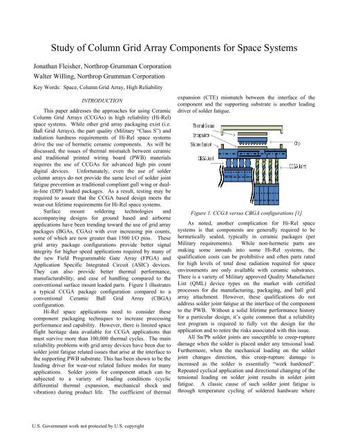
Study of Ball Grid and Column Grid Array
Study of Ball Grid and Column Grid Array
Study of Ball Grid and Column Grid Array

Create successful ePaper yourself
Turn your PDF publications into a flip-book with our unique Google optimized e-Paper software.
<strong>Study</strong> <strong>of</strong> <strong>Column</strong> <strong>Grid</strong> <strong>Array</strong> Components for Space Systems<br />
Jonathan Fleisher, Northrop Grumman Corporation<br />
Walter Willing, Northrop Grumman Corporation<br />
Key Words: Space, <strong>Column</strong> <strong>Grid</strong> <strong>Array</strong>, High Reliability<br />
INTRODUCTION<br />
This paper addresses the approaches for using Ceramic<br />
<strong>Column</strong> <strong>Grid</strong> <strong>Array</strong>s (CCGAs) in high reliability (Hi-Rel)<br />
space systems. While other grid array packaging exist (i.e.<br />
<strong>Ball</strong> <strong>Grid</strong> <strong>Array</strong>s), the part quality (Military “Class S”) <strong>and</strong><br />
radiation hardness requirements <strong>of</strong> Hi-Rel space systems<br />
drive the use <strong>of</strong> hermetic ceramic components. As will be<br />
discussed, the issues <strong>of</strong> thermal mismatch between ceramic<br />
<strong>and</strong> traditional printed wiring board (PWB) materials<br />
requires the use <strong>of</strong> CCGAs for advanced high pin count<br />
digital devices. Unfortunately, even the use <strong>of</strong> solder<br />
column arrays do not provide the same level <strong>of</strong> solder joint<br />
fatigue prevention as traditional compliant gull wing or dualin-line<br />
(DIP) leaded packages. As a result, testing may be<br />
required to assure that the CCGA based design meets the<br />
wear-out lifetime requirements for Hi-Rel space systems.<br />
Surface mount soldering technologies <strong>and</strong><br />
accompanying designs for ground based <strong>and</strong> airborne<br />
applications have been trending toward the use <strong>of</strong> grid array<br />
packages (BGAs, CGAs) with ever increasing pin counts,<br />
some <strong>of</strong> which are now greater than 1500 I/O pins. These<br />
grid array package configurations provide better signal<br />
integrity for higher speed applications required by many <strong>of</strong><br />
the new Field Programmable Gate <strong>Array</strong> (FPGA) <strong>and</strong><br />
Application Specific Integrated Circuit (ASIC) devices.<br />
They can also provide better thermal performance,<br />
manufacturability, <strong>and</strong> ease <strong>of</strong> h<strong>and</strong>ling compared to the<br />
conventional surface mount leaded parts. Figure 1 illustrates<br />
a typical CCGA package configuration compared to a<br />
conventional Ceramic <strong>Ball</strong> <strong>Grid</strong> <strong>Array</strong> (CBGA)<br />
configuration.<br />
Hi-Rel space applications need to consider these<br />
component packaging techniques to increase processing<br />
performance <strong>and</strong> capability. However, there is limited space<br />
flight heritage data available for CCGA applications that<br />
must survive more than 100,000 thermal cycles. The main<br />
reliability problems with grid array devices have been due to<br />
solder joint fatigue related issues that arise at the interface to<br />
the supporting PWB substrate. This has been shown to be the<br />
leading driver for wear-out related failure modes for many<br />
applications. Solder joints for component attach can be<br />
subjected to a variety <strong>of</strong> loading conditions (cyclic<br />
differential thermal expansion, mechanical shock <strong>and</strong><br />
vibration) during product life. The coefficient <strong>of</strong> thermal<br />
U.S. Government work not protected by U.S. copyright<br />
expansion (CTE) mismatch between the interface <strong>of</strong> the<br />
component <strong>and</strong> the supporting substrate is another leading<br />
driver <strong>of</strong> solder fatigue.<br />
Figure 1. CCGA versus CBGA configurations [1]<br />
As noted, another complication for Hi-Rel space<br />
systems is that components are generally required to be<br />
hermetically sealed, typically in ceramic packages (per<br />
Military requirements). While non-hermetic parts are<br />
making some inroads into some Hi-Rel systems, the<br />
qualification costs can be prohibitive <strong>and</strong> <strong>of</strong>ten parts rated<br />
for high levels <strong>of</strong> total dose radiation required for space<br />
environments are only available with ceramic substrates.<br />
There is a variety <strong>of</strong> Military approved Quality Manufacture<br />
List (QML) device types on the market with certified<br />
processes for die manufacturing, packaging, <strong>and</strong> ball grid<br />
array attachment. However, these qualifications do not<br />
address solder joint fatigue at the interface <strong>of</strong> the component<br />
to the PWB. Without a solid lifetime performance history<br />
for a particular design, it’s quite common that a reliability<br />
test program is required to fully vet the design for the<br />
application <strong>and</strong> to retire the risks associated with this issue.<br />
All Sn/Pb solder joints are susceptible to creep-rupture<br />
damage when the solder is placed under any tensional load.<br />
Furthermore, when the mechanical loading on the solder<br />
joint changes direction, this creep-rupture damage is<br />
increased as the solder is essentially “work hardened”.<br />
Repeated cyclical application <strong>and</strong> directional changing <strong>of</strong> the<br />
tensional loading on solder joint results in solder joint<br />
fatigue. A classic cause <strong>of</strong> such solder joint fatigue is<br />
through temperature cycling <strong>of</strong> soldered hardware where
there is a difference between the CTE for the part <strong>and</strong> the<br />
support substrate or PWB material. This difference in CTE<br />
is known as CTE mismatch. The combinations <strong>of</strong><br />
temperature changes, due to external environment or power<br />
switching, <strong>and</strong> materials that possess different CTEs,<br />
produce substantial cyclic strains within the solder.<br />
SOLDER JOINT FATIGUE<br />
For traditional leaded parts, either Gull Wing or DIP,<br />
any board-to-part CTE mismatch is <strong>of</strong>ten absorbed by the<br />
leads themselves when they are properly formed (known as<br />
“compliant leads”) <strong>and</strong> very little tension load is applied to<br />
the solder. A practical limit for leaded device pin count is<br />
approximately 300 to 350 pins. As noted, to support the<br />
increased I/O requirements <strong>of</strong> current state-<strong>of</strong>-the-art<br />
devices, grid arrays (BGAs, CGAs) have been developed.<br />
There is a fatigue concern with grid array attachment<br />
because the parts are essentially soldered directly to the<br />
PWB with minimal lead compliance to absorb the thermal<br />
strain developed by the CTE mismatch between the part <strong>and</strong><br />
the PWB. When comparing <strong>Ball</strong> <strong>Grid</strong> <strong>Array</strong>s to <strong>Column</strong><br />
<strong>Grid</strong> <strong>Array</strong>s, CGAs provide a more robust design for thermal<br />
cycling environments by two means<br />
• The solder columns are typically designed to have a<br />
lower stiffness than a solder ball (sphere).<br />
• The solder column provides a higher st<strong>and</strong><strong>of</strong>f distance<br />
between the component <strong>and</strong> the board.<br />
These two features enable the column leads to flex with<br />
less stress as the dimensional expansion between the<br />
component <strong>and</strong> the board varies. The taller st<strong>and</strong><strong>of</strong>f will<br />
reduce the stress in the solder joint by approximately the<br />
square <strong>of</strong> the distance between the component <strong>and</strong> the board<br />
[2].<br />
While CGAs have slightly higher “lead compliance”<br />
than BGAs, the extra lead compliance <strong>of</strong> the solder column<br />
for Ceramic CGAs is <strong>of</strong>ten <strong>of</strong>fset by the larger CTE<br />
mismatch. Figure 2 illustrates the forces applied to the<br />
solder joints resulting from CTE mismatch <strong>and</strong> thermal<br />
excursions <strong>and</strong> Figure 3 shows an actual failed column joint<br />
following temperature cycling.<br />
2.1. Improving Solder Joint Robustness<br />
Matching the CTE as closely as possible reduces cycling<br />
stress <strong>and</strong> improves the reliability <strong>of</strong> the joints. However,<br />
there are trade<strong>of</strong>fs between selecting the best CTE<br />
compatibility matches <strong>and</strong> electrical performance. Examples<br />
<strong>of</strong> CTEs for common materials are shown in Table 1.<br />
A method to improve CTE mismatch is to use<br />
compatible PWB materials with a CTE closer to the<br />
component CTE. One such PWB material is known as<br />
Thermount TM . Another PWB material is Stablecore TM .<br />
Conversely, one can also use a ceramic with a higher CTE<br />
than the typical alumina compounds (Hi-CTE Ceramic).<br />
Unfortunately, not all PWB vendors have qualified processes<br />
for the special materials, <strong>and</strong> not all components are<br />
available in the Hi-CTE ceramics. Additionally, there is<br />
Figure 2. Forces Applied to the solder joints [3]<br />
Figure 3. Example <strong>of</strong> a Failed <strong>Column</strong> <strong>Grid</strong> <strong>Array</strong> [4]<br />
Table 1. CTE for Common Materials[5]<br />
Material CTE ≈<br />
PLASTIC BGA 15 ppm/°C<br />
Ceramic BGA Material 6.7 ppm/°C<br />
Hi-CTE Ceramic 10 ppm/°C<br />
Polyimide PWB Material 16 ppm/°C<br />
<strong>of</strong>ten a mix <strong>of</strong> component styles on boards <strong>and</strong> the use <strong>of</strong> one<br />
combination can have adverse effects on the other<br />
combination <strong>of</strong> materials. There are also several kinds <strong>of</strong><br />
solder columns available in the industry. Some have copper
wire or foil within the columns to provide extra robustness<br />
(e.g. 6 Sigma TM solder columns). Figure 4 illustrates some<br />
<strong>of</strong> the features <strong>of</strong> a 6 Sigma TM solder column.<br />
Figure 4. 6 Sigma TM Solder <strong>Column</strong> Design<br />
2.2. Thermal cycle acceleration models <strong>and</strong> testing<br />
The fundamental physical issue with space systems is<br />
the extended operational mission pr<strong>of</strong>iles for each space<br />
system, <strong>of</strong>ten including over a hundred thous<strong>and</strong> thermal<br />
cycles before end-<strong>of</strong>-life (EOL). Space systems are exposed<br />
to thermal cycling from orbital changes, daily (diurnal)<br />
changes, sun angle changes, <strong>and</strong> power cycling. Since<br />
power consumption <strong>and</strong> mass are critical considerations,<br />
they are <strong>of</strong>ten continuously power cycled <strong>and</strong> the circuit<br />
board assemblies become a “thermal capacitor”, constantly<br />
heating <strong>and</strong> cooling.<br />
As the use <strong>of</strong> CGAs in space represents a wear-out<br />
condition, one means for underst<strong>and</strong>ing <strong>and</strong> mitigating the<br />
risk <strong>of</strong> using CGAs is through the use <strong>of</strong> thermal cycle life<br />
testing. The goal <strong>of</strong> the accelerated thermal cycle life testing<br />
is to determine the wear-out distribution for the CGA/PWB<br />
configuration. The resulting onset (e.g. 1% failure rate<br />
point) <strong>of</strong> the wear-out distribution should be greater than the<br />
expected number <strong>of</strong> temperature cycles predicted over life<br />
time operation with sufficient margin. Since testing for over<br />
100,000 thermal cycles is prohibitive from both a time <strong>and</strong><br />
cost perspective, accelerated temperature testing is required.<br />
To project an accelerated test to real life, acceleration models<br />
were developed. There are several widely known<br />
acceleration models used to project test thermal cycles to<br />
operational thermal cycles. Two specific models are [6],[7]:<br />
1. The Basic C<strong>of</strong>fin Manson Model:<br />
AF = (ΔTTEST / ΔTOPERATE) 2.5 (1)<br />
An exponent <strong>of</strong> 2.4 to 2.5 is used for Sn/Pb solder<br />
2. The C<strong>of</strong>fin-Manson-Norris-L<strong>and</strong>zburg Model:<br />
AF = [ΔTTEST/ΔTOPERATE] 2.0 (fOPERATE/fTEST) 1/3<br />
exp(1414{1/TmaxOPERATE - 1/TmaxTEST}) (2)<br />
where<br />
AF = Acceleration Factor<br />
ΔTTEST = Delta T in the Lab<br />
ΔTOPERATE = Delta T in the "Field" or "In Use"<br />
fOPERATE = Frequency <strong>of</strong> cycles in the field (i.e. 16<br />
Orbits / Day - LEO, 1 Orbit / Day GEO)<br />
fTEST = Frequency <strong>of</strong> test cycles in the lab (i.e. 24 test<br />
cycles / day)<br />
TmaxOPERATE = Maximum Temperature in the field<br />
TmaxTEST = Maximum Temperature in the lab<br />
The C<strong>of</strong>fin-Manson-Norris-L<strong>and</strong>zburg model addresses<br />
temperature dwell times <strong>and</strong> the absolute temperature within<br />
the range <strong>of</strong> the operational <strong>and</strong> thermal cycling, but it tends<br />
to be more conservative than the Basic C<strong>of</strong>fin Manson<br />
Model. The acceleration factor (AF) for using both<br />
equations, as applied to a 5-year space mission, is shown in<br />
Table 2. The specific “Life” delta temperature ranges <strong>and</strong><br />
life cycle quantities are determined from examining the<br />
thermal mission pr<strong>of</strong>ile for a typical “Day In the Life” for the<br />
equipment <strong>of</strong> interest. There are four “life” delta<br />
temperature ranges shown with their quantities <strong>and</strong> expected<br />
cycles. Table 2 also shows the results <strong>of</strong> the 2x <strong>and</strong> 3x<br />
margins as applied to Basic C<strong>of</strong>fin Manson <strong>and</strong> C<strong>of</strong>fin-<br />
Manson-Norris-L<strong>and</strong>zburg model results. It should be noted<br />
that a minimum 2x margin should be applied no matter what<br />
the case to account for any unforeseen affects.<br />
2.3. Life test accuracy <strong>and</strong> margin<br />
Several vendors have used similar models to evaluate<br />
their CGA designs [8],[9]. Despite the prevalent use <strong>of</strong> these<br />
acceleration models, a wide variability <strong>of</strong> acceleration results<br />
exist for cases where the accelerated test results have been<br />
compared to the actual measured thermal cycle fatigue life<br />
(wear-out life). Figure 5 reveals this variability. As shown<br />
in the graph, there is a noticeable degree <strong>of</strong> variation<br />
between the observed <strong>and</strong> the predicted acceleration factors.<br />
Figure 5. Predicted <strong>and</strong> Observed Thermal Cycle<br />
Acceleration Model results [11]
Based on review <strong>of</strong> test data versus the predicted values,<br />
the true acceleration factors (AF) vary from one-half to twice<br />
the predicted acceleration factors. To mitigate this<br />
accelerated test variability, it is recommended that a three to<br />
four fold margin be applied to the accelerated life results.<br />
2.4. Recommendations for cga thermal cycle life testing<br />
There are several recommendations for CGA<br />
thermal cycle life testing. These recommendations are<br />
advised for any accelerated life test. One <strong>of</strong> the most<br />
important (especially for larger CGA styles) is that thermal<br />
cycle life testing be performed for each CGA style mounted<br />
to a PWB that represents the final configuration to the<br />
maximum extent possible. The life testing should use the<br />
exact package <strong>and</strong> board mounting configuration <strong>and</strong><br />
physical properties, including package size, internal die size,<br />
ball material size <strong>and</strong> pitch, solder mask, <strong>and</strong> PWB stack-up<br />
(thickness, layers, etc) used in the actual package. If the<br />
exact configurations cannot be tested, IPC-9701, Table 4-3<br />
(Test Exemption Requirements) can be used as a guide to<br />
determine the extent <strong>of</strong> the allowed configuration deviations.<br />
IPC-9701 should be used to define the life test conditions<br />
<strong>and</strong> required sample sizes. The accelerated life test thermal<br />
cycle pr<strong>of</strong>ile should be based upon initial startup conditions<br />
<strong>and</strong> the operational temperature levels anticipated at the<br />
components interconnection interfaces. The dwell duration<br />
at the extremes shall be a minimum <strong>of</strong> 15 minutes. This<br />
dwell time provides sufficient time for the solder to “creep”<br />
or deform under tensional load. Per IPC-9701, the sample<br />
size <strong>of</strong> each device type shall be 33 devices, 32 for life test<br />
<strong>and</strong> one for cross-section. All testing should be performed<br />
using “Daisy Chained” parts <strong>and</strong> PWB interconnections so<br />
that continuous continuity monitoring can be performed with<br />
an IPC approved event detector. The temperature rise from<br />
chip self heating should be reflected in the predicted thermal<br />
cycle numbers. Therefore, differences between the actual<br />
Table 2. Thermal Acceleration Model<br />
This margin provides a level <strong>of</strong> conservatism so that the<br />
variability can be discounted. Consultants for NASA<br />
specifically recommend applying a three-fold (3x) margin<br />
[10].<br />
chip <strong>and</strong> daisy chained chip need to be considered. The<br />
“Daisy Chained” parts should reflect the exact part<br />
configuration (size, materials, layer count, thickness), with<br />
the exception that the I/O be connected in a fashion allowing<br />
for a complete daisy chained interconnection to a properly<br />
designed daisy chained PWB. The corresponding Daisy<br />
chain PWB design should have the same copper <strong>and</strong><br />
insulating layer stack up as the actual board design, again<br />
with the exception that the circuitry connection to the parts<br />
be designed to have continuous daisy chained continuity<br />
loops. The resulting PWB <strong>and</strong> component assembly should<br />
be performed using the identical soldering <strong>and</strong> assembly<br />
processes as the final product.<br />
2.5. Space program CGA thermal life testing<br />
The following is an example <strong>of</strong> a CGA evaluation test.<br />
As illustrated in Table 2, a Day-In-The-Life thermal cycle<br />
mission pr<strong>of</strong>ile was created. Using the Basic C<strong>of</strong>fin<br />
equation, an equivalent accelerated life test value <strong>of</strong> 251<br />
cycles (-40°C to +95°C) was computed as the “1x” lifetime<br />
value (no margin). The application required a “3x” margin<br />
for wear-out distributions, therefore, the resulting CGA<br />
thermal life test cycle requirement was determined to be 754<br />
cycles. The complete mission pr<strong>of</strong>ile includes contributions<br />
from manufacturing/screening, Integration/Test <strong>and</strong> on-orbit<br />
“life” temperature cycling as shown in Table 2.<br />
An Event Detector (Analysis Tech TM , STD Series)<br />
monitored each solder joint during test. The test boards<br />
began to show CGA failures (open circuits) at 879 test cycles<br />
(refer to Table 3). The primary objective <strong>of</strong> the test program<br />
followed by the Weibull analysis is to determine the <strong>Column</strong>
<strong>Grid</strong> <strong>Array</strong> (CGA) life. As noted, the time to first Failure<br />
was 879 Test Cycles. However, an important criterion is the<br />
1% failure point on a Weibull plot as shown in Figure 6. For<br />
the full set <strong>of</strong> data, the 1% failure point was 740 Cycles.<br />
Table 3. Test Board Results<br />
However, careful analysis <strong>of</strong> the data revealed dual slopes,<br />
which indicates a Bi-Modal distribution. Confidence <strong>of</strong> the<br />
dual slopes is confirmed by the fact that the Coefficient <strong>of</strong><br />
Determination (r^2) factors <strong>of</strong> the individual data plots are<br />
higher than the combined plot, <strong>and</strong> the early failure mode<br />
plot has an extremely high Coefficient <strong>of</strong> Determination<br />
value <strong>of</strong> 0.95. Since the time to first failure is the most<br />
important, only the earliest failure mode distribution is used<br />
to determine the minimum design life. Plotting the earliest<br />
failure mode distribution shows a beta ( ) <strong>of</strong> 30.1, which is<br />
O<br />
c<br />
c<br />
u<br />
r<br />
r<br />
e<br />
n<br />
c<br />
e<br />
C<br />
D<br />
F<br />
%<br />
O<br />
c<br />
c<br />
u<br />
r<br />
r<br />
e<br />
n<br />
c<br />
e<br />
C<br />
D<br />
F<br />
%<br />
“Early” Failure Distribution<br />
820 Cycles<br />
1% Failure Point<br />
Thermal Cycles<br />
strongly indicative <strong>of</strong> a wear-out related phenomenon.<br />
Since the 1% point <strong>of</strong> 820 test cycles was above the 754<br />
cycle goal, the life requirement (with a 3x margin) was<br />
satisfied <strong>and</strong> the overall design was deemed suitable for its<br />
application.<br />
2.6. Other test programs <strong>and</strong> studies<br />
In recent years, various board level thermal cycling<br />
qualification programs have been conducted by several<br />
device vendors. Two notable test programs were performed<br />
by Xilinx <strong>and</strong> Actel Corporations in support <strong>of</strong> their CGA<br />
designs. Although those test programs showed mixed results<br />
that varied depending on the given configurations, both test<br />
programs indicted the CGA designs have the capability to<br />
meet the needs for many space programs [12],[13].<br />
CONCLUSION<br />
A good reliability test program to evaluate solder joint<br />
fatigue risks should be implemented with the goal <strong>of</strong><br />
confirming the design meets the service life requirements <strong>of</strong><br />
the application. In particular, it should be focused on<br />
reflecting the lifetime temperature cycling exposure the<br />
equipment is expected to experience across the expected life.<br />
Subsequently, the environment <strong>and</strong> design life requirements<br />
must be fully analyzed <strong>and</strong> understood up front. An<br />
accelerated life test can be effectively designed using the<br />
Basic C<strong>of</strong>fin Manson model. This approach can be used to<br />
derive acceleration factors to use in designing a robust test<br />
program.<br />
Full Data Set Indicates Two Independent Failure Modes<br />
740 Cycles<br />
1% Failure Point<br />
Thermal Cycles<br />
Eta Beta r^2<br />
962 30.1 0.95<br />
REFERENCES<br />
Figure 6. Weibull Plotted Test Data<br />
Electronics”, 2000.<br />
1.<br />
2.<br />
Davis, William; “CGA: A Modified COTS Approach<br />
for Area <strong>Array</strong> Packaging <strong>of</strong> Military <strong>and</strong> Space<br />
Winslow, Russell T.; “Converting BGA Components to<br />
CGA” MASH Packaging Issues & Applications (MASH<br />
2005) Workshop.<br />
O<br />
c<br />
c<br />
u<br />
r<br />
r<br />
e<br />
n<br />
c<br />
e<br />
C<br />
D<br />
F<br />
%<br />
Eta Beta r^2<br />
1083 12 0.912<br />
Thermal Cycles<br />
Eta Beta r^2<br />
1156 21.4 0.914
3. Russell, 2<br />
4. Kuang, Raymond; “ Thermal Cycling Test Report for<br />
CCGA”, Actel Corp.<br />
5. Puttlitz, Karl;“Area <strong>Array</strong> Interconnection<br />
h<strong>and</strong>book”,Kluwer Academic Publishers, 2001<br />
6. SAE Aerospace, “Guideline for Preparing Reliability<br />
Assessment Plans for Electronic Engine Controls”,<br />
ARP5890A, 2011<br />
7. N. Pan et al, “An Acceleration Model for Sn-Ag-Cu<br />
Solder Joint Reliability Under Various Thermal Cycle<br />
Conditions”pp.876-883, SMTAI, Sept 2005, Chicago,<br />
IL<br />
8. Roosta, Ramin; “Xilinx Virtex-4 FPGAs for Space<br />
Applications”, JPL, Pasadena, Ca, Dec, 2009.<br />
9. Kuang, p. 2<br />
10. Ghaffarian, Reza;“Qualification approaches <strong>and</strong> thermal<br />
cycle test results for CSP/BGA/FCBGA”,<br />
Microelectronics Reliability 43 (2003)<br />
11. Hillman, C; “Pb-Free Norris-L<strong>and</strong>zberg Model to JG-PP<br />
Test Data”, DFR Solutions, 2006.<br />
12. Roosta, p. 4<br />
13. Kuang, p. 2<br />
BIOGRAPHIES<br />
Jonathan Fleisher<br />
Northrop Grumman Corporation<br />
7323 Aviation Blvd,<br />
Baltimore, MD, 21090, USA<br />
e-mail: jonathan.fleisher@ngc.com<br />
Mr. Fleisher is a Reliability Engineer within the Northrop<br />
Grumman Corp Electronic Systems Sector, System<br />
Supportability Engineering Department. Mr. Fleisher<br />
received a BSME <strong>and</strong> an MSIE from New Mexico State<br />
University. He has 16 years <strong>of</strong> engineering experience on a<br />
variety <strong>of</strong> defense related programs.<br />
Walter Willing<br />
Northrop Grumman Corporation<br />
7323 Aviation Blvd,<br />
Baltimore, MD, 21090, USA<br />
e-mail: walter.willing@ngc.com<br />
Mr. Willing is a Senior Advisory Reliability Engineer within<br />
the Northrop Grumman Corp Electronic Systems Sector,<br />
System Supportability Engineering Department. Mr. Willing<br />
has over 30 years experience in space systems reliability. He<br />
received a BSEE from the University <strong>of</strong> Delaware <strong>and</strong> an<br />
MSEE from the Loyola College <strong>of</strong> Maryl<strong>and</strong>.