

M2110 Hardware Reference Manual - MEMSIC
M2110 Hardware Reference Manual - MEMSIC
M2110 Hardware Reference Manual - MEMSIC

Create successful ePaper yourself
Turn your PDF publications into a flip-book with our unique Google optimized e-Paper software.
4 IRIS OEM <strong>Reference</strong> Board<br />
IRIS OEM Edition <strong>Hardware</strong> <strong>Reference</strong> <strong>Manual</strong><br />
The IRIS OEM reference board is a carrier PCB with the same form factor and functionality as<br />
the IRIS family product. It consists of a surface mount module consisting of a processor core<br />
and a two-way radio, high density digital interface connector, RF coaxial antenna connector,<br />
power supply connection, battery pack connection, power switch, and mounting holes.<br />
4.1 Block Diagram<br />
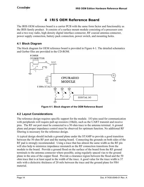
The block diagram for OEM reference board is provided in Figure 4-1. The detailed schematics<br />
and Gerber files are provided in the CD-ROM.<br />
4.2 Layout Considerations<br />
Figure 4-1. Block diagram of the OEM <strong>Reference</strong> Board<br />
The reference design requires specific support for the module. I/O pins used for communication<br />
with peripherals will require pull-up resistors (10kΩ), such as the UART transmit and receive<br />
pins. The RF out port must be connected to a 50 ohm trace to the antenna terminal. A ground<br />
plane and proper impedance control must be observed for optimum function. No additional RF<br />
filtering is necessary for the reference design.<br />
A typical design should include a ground plane under the STAMP to provide a good transition<br />
between the 50 ohm RF port and the mating board. Connecting the grounds on both sides of the<br />
RF pad is strongly recommended. Using a trace that has almost the same width as the RF pin<br />
will also help to minimize impedance mismatch as the RF connection transitions from the<br />
module to the board. Provide a ground flood on the surface of the board from the RF ground<br />
terminals to the antenna connector where possible, using regularly spaced vias to the ground<br />
plane in the area of the copper flood. Provide a clearance region between the flood and the 50<br />
ohm trace that is at least equal to the width of the trace. A good value for the trace width is 37<br />
mils with a dielectric thickness of 20 mils between the trace and the ground plane for FR4<br />
material.<br />
Page 14 Doc. # 7430-0549-01 Rev. A