NSI45025 - CCR & LED Driver - Silica
NSI45025 - CCR & LED Driver - Silica
NSI45025 - CCR & LED Driver - Silica

Create successful ePaper yourself
Turn your PDF publications into a flip-book with our unique Google optimized e-Paper software.
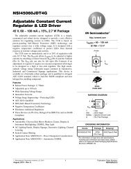
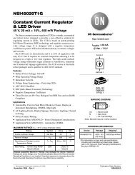
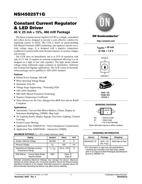
<strong>NSI45025</strong>T1G<br />
Constant Current Regulator<br />
& <strong>LED</strong> <strong>Driver</strong><br />
45 V, 25 mA 15%, 460 mW Package<br />
The linear constant current regulator (<strong>CCR</strong>) is a simple, economical<br />
and robust device designed to provide a cost−effective solution for<br />
regulating current in <strong>LED</strong>s. The <strong>CCR</strong> is based on patent-pending<br />
Self-Biased Transistor (SBT) technology and regulates current over a<br />
wide voltage range. It is designed with a negative temperature<br />
coefficient to protect <strong>LED</strong>s from thermal runaway at extreme voltages<br />
and currents.<br />
The <strong>CCR</strong> turns on immediately and is at 25% of regulation with<br />
only 0.5 V Vak. It requires no external components allowing it to be<br />
designed as a high or low−side regulator. The high anode-cathode<br />
voltage rating withstands surges common in Automotive, Industrial<br />
and Commercial Signage applications. The <strong>CCR</strong> comes in thermally<br />
robust packages and is qualified to AEC-Q101 standard.<br />
Features<br />
• Robust Power Package: 460 mW<br />
• Wide Operating Voltage Range<br />
• Immediate Turn-On<br />
• Voltage Surge Suppressing − Protecting <strong>LED</strong>s<br />
• AEC-Q101 Qualified<br />
• SBT (Self−Biased Transistor) Technology<br />
• Negative Temperature Coefficient<br />
• These Devices are Pb−Free, Halogen Free/BFR Free and are RoHS<br />
Compliant<br />
Applications<br />
• Automobile: Chevron Side Mirror Markers, Cluster, Display &<br />
Instrument Backlighting, CHMSL, Map Light<br />
• AC Lighting Panels, Display Signage, Decorative Lighting, Channel<br />
Lettering<br />
• Switch Contact Wetting<br />
• Application Note AND8391/D − Power Dissipation Considerations<br />
• Application Note AND8349/D − Automotive CHMSL<br />
MAXIMUM RATINGS (TA = 25°C unless otherwise noted)<br />
Rating Symbol Value Unit<br />
Anode−Cathode Voltage Vak Max 45 V<br />
Reverse Voltage V R 500 mV<br />
Operating and Storage Junction<br />
Temperature Range<br />
ESD Rating: Human Body Model<br />
Machine Model<br />
© Semiconductor Components Industries, LLC, 2009<br />
November, 2009 − Rev. 3<br />
T J, T stg −55 to +150 °C<br />
ESD Class 1C<br />
Class B<br />
Stresses exceeding Maximum Ratings may damage the device. Maximum<br />
Ratings are stress ratings only. Functional operation above the Recommended<br />
Operating Conditions is not implied. Extended exposure to stresses above the<br />
Recommended Operating Conditions may affect device reliability.<br />
http://onsemi.com<br />
Ireg(SS) = 25 mA<br />
@ Vak = 7.5 V<br />
Anode 2<br />
Cathode 1<br />
SOD−123<br />
CASE 425<br />
STYLE 1<br />
MARKING DIAGRAM<br />
AE M <br />
1 2<br />
<br />
AE = Device Code<br />
M = Date Code<br />
= Pb−Free Package<br />
(Note: Microdot may be in either location)<br />
ORDERING INFORMATION<br />
Device Package Shipping †<br />
<strong>NSI45025</strong>T1G SOD−123<br />
(Pb−Free)<br />
1<br />
3000/Tape & Reel<br />
†For information on tape and reel specifications,<br />
including part orientation and tape sizes, please<br />
refer to our Tape and Reel Packaging Specifications<br />
Brochure, BRD8011/D.<br />
1 Publication Order Number:<br />
<strong>NSI45025</strong>/D<br />
2
<strong>NSI45025</strong>T1G<br />
ELECTRICAL CHARACTERISTICS (TA = 25°C unless otherwise noted)<br />
Characteristic Symbol Min Typ Max Unit<br />
Steady State Current @ Vak = 7.5 V (Note 1) Ireg(SS) 21.25 25 28.75 mA<br />
Voltage Overhead (Note 2) Voverhead 1.8 V<br />
Pulse Current @ Vak = 7.5 V (Note 3) Ireg(P) 24.4 29.4 34.5 mA<br />
Capacitance @ Vak = 7.5 V (Note 4) C 2.5 pF<br />
Capacitance @ Vak = 0 V (Note 4) C 5.7 pF<br />
1. Ireg(SS) steady state is the voltage (Vak) applied for a time duration ≥ 10 sec, using FR−4 @ 300 mm2 1 oz. Copper traces, in still air.<br />
2. Voverhead = Vin − V<strong>LED</strong>s. Voverhead is typical value for 80% Ireg(SS). 3. Ireg(P) non−repetitive pulse test. Pulse width t ≤ 300 sec.<br />
4. f = 1 MHz, 0.02 V RMS.<br />
THERMAL CHARACTERISTICS<br />
Total Device Dissipation (Note 5) T A = 25°C<br />
Derate above 25°C<br />
Characteristic Symbol Max Unit<br />
http://onsemi.com<br />
2<br />
P D<br />
208<br />
1.66<br />
mW<br />
mW/°C<br />
Thermal Resistance, Junction−to−Ambient (Note 5) RθJA 600 °C/W<br />
Thermal Reference, Lead−to−Ambient (Note 5) RψLA 404 °C/W<br />
Thermal Reference, Junction−to−Cathode Lead (Note 5) RψJL 196 °C/W<br />
Total Device Dissipation (Note 6) T A = 25°C<br />
Derate above 25°C<br />
P D<br />
227<br />
1.8<br />
mW<br />
mW/°C<br />
Thermal Resistance, Junction−to−Ambient (Note 6) RθJA 550 °C/W<br />
Thermal Reference, Lead−to−Ambient (Note 6) RψLA 390 °C/W<br />
Thermal Reference, Junction−to−Cathode Lead (Note 6) RψJL 160 °C/W<br />
Total Device Dissipation (Note 7) T A = 25°C<br />
Derate above 25°C<br />
P D<br />
347<br />
2.8<br />
mW<br />
mW/°C<br />
Thermal Resistance, Junction−to−Ambient (Note 7) RθJA 360 °C/W<br />
Thermal Reference, Lead−to−Ambient (Note 7) RψLA 200 °C/W<br />
Thermal Reference, Junction−to−Cathode Lead (Note 7) RψJL 160 °C/W<br />
Total Device Dissipation (Note 8) T A = 25°C<br />
Derate above 25°C<br />
P D<br />
368<br />
2.9<br />
mW<br />
mW/°C<br />
Thermal Resistance, Junction−to−Ambient (Note 8) RθJA 340 °C/W<br />
Thermal Reference, Lead−to−Ambient (Note 8) RψLA 208 °C/W<br />
Thermal Reference, Junction−to−Cathode Lead (Note 8) RψJL 132 °C/W<br />
Total Device Dissipation (Note 9) T A = 25°C<br />
Derate above 25°C<br />
P D<br />
436<br />
3.5<br />
mW<br />
mW/°C<br />
Thermal Resistance, Junction−to−Ambient (Note 9) RθJA 287 °C/W<br />
Thermal Reference, Lead−to−Ambient (Note 9) RψLA 139 °C/W<br />
Thermal Reference, Junction−to−Cathode Lead (Note 9) RψJL 148 °C/W<br />
Total Device Dissipation (Note 10) T A = 25°C<br />
Derate above 25°C<br />
P D<br />
463<br />
3.7<br />
mW<br />
mW/°C<br />
Thermal Resistance, Junction−to−Ambient (Note 10) RθJA 270 °C/W<br />
Thermal Reference, Lead−to−Ambient (Note 10) RψLA 150 °C/W<br />
Thermal Reference, Junction−to−Cathode Lead (Note 10) RψJL 120 °C/W<br />
Junction and Storage Temperature Range T J, T stg −55 to +150 °C<br />
5. FR−4 @ 100 mm2 , 1 oz. copper traces, still air.<br />
6. FR−4 @ 100 mm2 , 2 oz. copper traces, still air.<br />
7. FR−4 @ 300 mm2 , 1 oz. copper traces, still air.<br />
8. FR−4 @ 300 mm2 , 2 oz. copper traces, still air.<br />
9. FR−4 @ 500 mm2 , 1 oz. copper traces, still air.<br />
10.FR−4 @ 500 mm2 , 2 oz. copper traces, still air.<br />
NOTE: Lead measurements are made by non−contact methods such as IR with treated surface to increase emissivity to 0.9.<br />
Lead temperature measurement by attaching a T/C may yield values as high as 30% higher °C/W values based upon empirical<br />
measurements and method of attachment.
I reg, CURRENT REGULATION (mA)<br />
I reg(P), PULSE CURRENT (mA)<br />
I reg, CURRENT REGULATION (mA)<br />
60<br />
50<br />
40<br />
30<br />
20<br />
10<br />
0<br />
−10<br />
−20<br />
−10<br />
31<br />
30<br />
29<br />
28<br />
27<br />
26<br />
25<br />
3.0<br />
30<br />
29<br />
28<br />
27<br />
26<br />
25<br />
24<br />
0<br />
VR<br />
0<br />
<strong>NSI45025</strong>T1G<br />
TYPICAL PERFORMANCE CURVES<br />
Minimum FR−4 @ 300 mm 2 , 1 oz Copper Trace, Still Air<br />
Figure 1. General Performance Curve for <strong>CCR</strong> Figure 2. Steady State Current (I reg(SS)) vs.<br />
Anode−Cathode Voltage (Vak)<br />
4.0<br />
5<br />
10<br />
5.0<br />
6.0<br />
Non−Repetitive Pulse Test<br />
7.0<br />
8.0<br />
Vak, ANODE−CATHODE VOLTAGE (V) I reg(P), PULSE CURRENT (mA)<br />
Figure 3. Pulse Current (I reg(P)) vs.<br />
Anode−Cathode Voltage (Vak)<br />
10<br />
20 30 40 50 60<br />
Vak, ANODE−CATHODE VOLTAGE (V)<br />
TIME (s)<br />
T A = 25°C<br />
9.0<br />
Vak @ 7.5 V<br />
T A = 25°C<br />
Figure 5. Current Regulation vs. Time<br />
10<br />
15 20 25 30 35<br />
I reg(SS), STEADY STATE CURRENT (mA)<br />
I reg(SS), STEADY STATE CURRENT (mA)<br />
POWER DISSIPATION (mW)<br />
35<br />
30<br />
25<br />
20<br />
15<br />
10<br />
5<br />
0<br />
0<br />
29<br />
28<br />
27<br />
26<br />
25<br />
24<br />
23<br />
22<br />
21<br />
24<br />
800<br />
700<br />
300<br />
200<br />
100<br />
−40<br />
http://onsemi.com<br />
3<br />
1<br />
Vak @ 7.5 V<br />
TA = 25°C<br />
25<br />
26<br />
27 28 29 30 31 32 33 34 35<br />
Figure 4. Steady State Current vs. Pulse<br />
Current Testing<br />
500 mm 2 /2 oz<br />
600<br />
500 mm<br />
500<br />
2 /1 oz<br />
300 mm2 300 mm<br />
400 /1 oz<br />
2 /2 oz<br />
100 mm 2 /1 oz<br />
Vak, ANODE−CATHODE VOLTAGE (V)<br />
−20<br />
2<br />
T A = −40°C<br />
T A = 25°C<br />
T A = 85°C<br />
3<br />
0<br />
4<br />
DC Test Steady State, Still Air<br />
100 mm 2 /2 oz<br />
20<br />
5<br />
−0.061 mA/°C<br />
typ @ Vak = 7.5 V<br />
40<br />
60<br />
T A, AMBIENT TEMPERATURE (°C)<br />
7 8 9 10<br />
Figure 6. Power Dissipation vs. Ambient<br />
Temperature @ T J = 150C<br />
6<br />
−0.055 mA/°C<br />
typ @ Vak = 7.5 V<br />
80
APPLICATIONS<br />
+<br />
−<br />
V in<br />
<strong>NSI45025</strong>T1G<br />
D1 D1<br />
Anode<br />
Cathode<br />
Q1 Q2<br />
<strong>LED</strong><br />
HF3−R5570<br />
<strong>LED</strong><br />
HF3−R5570<br />
<strong>LED</strong><br />
HF3−R5570<br />
<strong>LED</strong><br />
HF3−R5570<br />
<strong>LED</strong><br />
HF3−R5570<br />
<strong>LED</strong><br />
HF3−R5570<br />
Figure 7. Typical Application Circuit<br />
(25 mA each <strong>LED</strong> String)<br />
Qx<br />
<strong>LED</strong><br />
HF3−R5570<br />
<strong>LED</strong><br />
HF3−R5570<br />
<strong>LED</strong><br />
HF3−R5570<br />
Number of <strong>LED</strong>’s that can be connected is determined by:<br />
D1 is a reverse battery protection diode<br />
<strong>LED</strong>’s = ((V in − Q X V F + D1 V F)/<strong>LED</strong> V F)<br />
Example: V in = 12 Vdc, Q X V F = 3.5 Vdc, D1VF = 0.7 V<br />
<strong>LED</strong> V F = 2.2 Vdc @ 25 mA<br />
(12 Vdc − 4.2 Vdc)/2.2 Vdc = 3 <strong>LED</strong>s in series.<br />
http://onsemi.com<br />
4<br />
+<br />
−<br />
V in<br />
Anode<br />
Cathode<br />
Q1 Q2<br />
<strong>LED</strong><br />
HF3−R5570<br />
<strong>LED</strong><br />
HF3−R5570<br />
<strong>LED</strong><br />
HF3−R5570<br />
Figure 8. Typical Application Circuit<br />
(75 mA each <strong>LED</strong> String)<br />
Number of <strong>LED</strong>’s that can be connected is determined by:<br />
D1 is a reverse battery protection diode<br />
Example: V in = 12 Vdc, Q X V F = 3.5 Vdc, D1VF = 0.7 V<br />
<strong>LED</strong> V F = 2.6 Vdc @ 75 mA<br />
(12 Vdc − (3.5 + 0.7 Vdc))/2.6 Vdc = 3 <strong>LED</strong>s in series.<br />
Number of <strong>Driver</strong>s = <strong>LED</strong> current/25 mA<br />
75 mA/25 mA = 3 <strong>Driver</strong>s (Q1, Q2, Q3)<br />
Qx
I (mA)<br />
<strong>NSI45025</strong>T1G<br />
Comparison of <strong>LED</strong> Circuit using <strong>CCR</strong> vs. Resistor Biasing<br />
ON Semiconductor <strong>CCR</strong> Design Resistor Biased Design<br />
Constant brightness over full Automotive Supply Voltage<br />
(more efficient), see Figure 9<br />
http://onsemi.com<br />
5<br />
Large variations in brightness over full Automotive Supply Voltage<br />
Little variation of power in <strong>LED</strong>s, see Figure 10 Large variations of current (power) in <strong>LED</strong>s<br />
Constant current extends <strong>LED</strong> strings lifetime, see Figure 9 High Supply Voltage/ Higher Current in <strong>LED</strong> strings limits lifetime<br />
Current decreases as voltage increases, see Figure 9 Current increases as voltage increases<br />
Current supplied to <strong>LED</strong> string decreases as temperature<br />
increases (self-limiting), see Figure 2<br />
35<br />
30<br />
25<br />
20<br />
15<br />
10<br />
9<br />
<strong>LED</strong> current decreases as temperature increases<br />
No resistors needed Requires costly inventory<br />
(need for several resistor values to match <strong>LED</strong> intensity)<br />
Fewer components, less board space required More components, more board space required<br />
T A = 25°C<br />
Circuit Current with<br />
<strong>CCR</strong> Device<br />
Circuit Current<br />
with 300 <br />
10<br />
Surface mount component Through-hole components<br />
11<br />
12<br />
Representative Test Data<br />
for Figure 7 Circuit, Current<br />
of <strong>LED</strong>s, FR−4 @ 300 mm 2 ,<br />
1 oz Copper Area<br />
13<br />
14<br />
15<br />
16<br />
<strong>LED</strong> Power<br />
100 with 300 Representative Test Data<br />
for Figure 7 Circuit, Pd of<br />
80<br />
<strong>LED</strong>s, FR−4 @ 300 mm<br />
9 10 11 12 13 14 15 16<br />
2 ,<br />
1 oz Copper Area<br />
60<br />
V in (V) V in (V)<br />
Figure 9. Series Circuit Current Figure 10. <strong>LED</strong> Power<br />
Current Regulation: Pulse Mode (I reg(P)) vs DC<br />
Steady-State (I reg(SS))<br />
There are two methods to measure current regulation:<br />
Pulse mode (Ireg(P)) testing is applicable for factory and<br />
incoming inspection of a <strong>CCR</strong> where test times are a<br />
minimum. (t < 300 s). DC Steady-State (Ireg(SS)) testing is<br />
applicable for application verification where the <strong>CCR</strong> will<br />
be operational for seconds, minutes, or even hours. ON<br />
Semiconductor has correlated the difference in Ireg(P) to<br />
Pd <strong>LED</strong>s (mW)<br />
200<br />
180<br />
160<br />
140<br />
120<br />
T A = 25°C<br />
<strong>LED</strong> Power with<br />
<strong>CCR</strong> Device<br />
Ireg(SS) for stated board material, size, copper area and<br />
copper thickness. Ireg(P) will always be greater than Ireg(SS)<br />
due to the die temperature rising during Ireg(SS). This heating<br />
effect can be minimized during circuit design with the<br />
correct selection of board material, metal trace size and<br />
weight, for the operating current, voltage, board operating<br />
temperature (TA) and package. (Refer to Thermal<br />
Characteristics table).
H E<br />
D<br />
1<br />
ÂÂÂÂ<br />
ÂÂÂÂ<br />
E<br />
2<br />
b<br />
C<br />
ÉÉ<br />
ÉÉ<br />
ÉÉ<br />
<strong>NSI45025</strong>T1G<br />
PACKAGE DIMENSIONS<br />
A<br />
SOD−123<br />
CASE 425−04<br />
ISSUE E<br />
A1<br />
L<br />
SOLDERING FOOTPRINT*<br />
0.91<br />
0.036<br />
2.36<br />
0.093<br />
4.19<br />
0.165<br />
ÉÉ<br />
ÉÉ<br />
ÉÉ<br />
SCALE 10:1<br />
http://onsemi.com<br />
6<br />
NOTES:<br />
1. DIMENSIONING AND TOLERANCING PER ANSI<br />
Y14.5M, 1982.<br />
2. CONTROLLING DIMENSION: INCH.<br />
mm<br />
inches <br />
*For additional information on our Pb−Free strategy and soldering<br />
details, please download the ON Semiconductor Soldering and<br />
Mounting Techniques Reference Manual, SOLDERRM/D.<br />
MILLIMETERS INCHES<br />
DIM MIN NOM MAX MIN NOM MAX<br />
A 0.94 1.17 1.35 0.037 0.046 0.053<br />
A1 0.00 0.05 0.10 0.000 0.002 0.004<br />
b 0.51 0.61 0.71 0.020 0.024 0.028<br />
c --- --- 0.15 --- --- 0.006<br />
D 1.40 1.60 1.80 0.055 0.063 0.071<br />
E 2.54 2.69 2.84 0.100 0.106 0.112<br />
HE 3.56 3.68 3.86 0.140 0.145 0.152<br />
L<br />
STYLE 1:<br />
0.25 --- --- 0.010 --- ---<br />
PIN 1. CATHODE<br />
2. ANODE<br />
1.22<br />
0.048<br />
ON Semiconductor and are registered trademarks of Semiconductor Components Industries, LLC (SCILLC). SCILLC reserves the right to make changes without further notice<br />
to any products herein. SCILLC makes no warranty, representation or guarantee regarding the suitability of its products for any particular purpose, nor does SCILLC assume any liability<br />
arising out of the application or use of any product or circuit, and specifically disclaims any and all liability, including without limitation special, consequential or incidental damages.<br />
“Typical” parameters which may be provided in SCILLC data sheets and/or specifications can and do vary in different applications and actual performance may vary over time. All<br />
operating parameters, including “Typicals” must be validated for each customer application by customer’s technical experts. SCILLC does not convey any license under its patent rights<br />
nor the rights of others. SCILLC products are not designed, intended, or authorized for use as components in systems intended for surgical implant into the body, or other applications<br />
intended to support or sustain life, or for any other application in which the failure of the SCILLC product could create a situation where personal injury or death may occur. Should Buyer<br />
purchase or use SCILLC products for any such unintended or unauthorized application, Buyer shall indemnify and hold SCILLC and its officers, employees, subsidiaries, affiliates,<br />
and distributors harmless against all claims, costs, damages, and expenses, and reasonable attorney fees arising out of, directly or indirectly, any claim of personal injury or death<br />
associated with such unintended or unauthorized use, even if such claim alleges that SCILLC was negligent regarding the design or manufacture of the part. SCILLC is an Equal<br />
Opportunity/Affirmative Action Employer. This literature is subject to all applicable copyright laws and is not for resale in any manner.<br />
PUBLICATION ORDERING INFORMATION<br />
LITERATURE FULFILLMENT:<br />
Literature Distribution Center for ON Semiconductor<br />
P.O. Box 5163, Denver, Colorado 80217 USA<br />
Phone: 303−675−2175 or 800−344−3860 Toll Free USA/Canada<br />
Fax: 303−675−2176 or 800−344−3867 Toll Free USA/Canada<br />
Email: orderlit@onsemi.com<br />
N. American Technical Support: 800−282−9855 Toll Free<br />
USA/Canada<br />
Europe, Middle East and Africa Technical Support:<br />
Phone: 421 33 790 2910<br />
Japan Customer Focus Center<br />
Phone: 81−3−5773−3850<br />
ON Semiconductor Website: www.onsemi.com<br />
Order Literature: http://www.onsemi.com/orderlit<br />
For additional information, please contact your local<br />
Sales Representative<br />
<strong>NSI45025</strong>/D