Applications - namlab
Applications - namlab
Applications - namlab

Create successful ePaper yourself
Turn your PDF publications into a flip-book with our unique Google optimized e-Paper software.
neu<br />
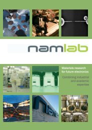
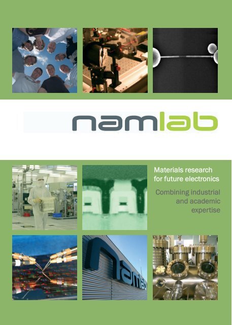
Materials research<br />
for future electronics<br />
Combining industrial<br />
g<br />
and academic<br />
expertise
NaMLab (Nano-electronic Materials Laboratory)<br />
The research at NaMLab focuses on materials<br />
for electronic devices and new device concepts.<br />
Among these are high-k materials for capacitors,<br />
transistors and other applications, novel<br />
switching devices including memristors,<br />
nanowire based electronics as well as materials<br />
for energy harvesting devices such as solar cells.<br />
Future nano-electronic products require the development of new<br />
materials that are not currently available. NaMLab consequently<br />
focuses its research activities on materials and applications that<br />
show the potential to offer significant advantages over materials<br />
and products used today today. In addition to investigating and<br />
characterizing new materials, NaMLab is undertaking research on<br />
the integration of these materials into semiconductor products<br />
with nano-scale dimensions.<br />
NaMLab, originally founded as a research joint venture between<br />
Qimonda AG and the TU Dresden in July 2006, has its roots in the<br />
Corporate Research Department of Infineon AG and is now owned<br />
completely by the Technical University of Dresden. NaMLab<br />
receives basic financing from the Saxon Ministry of Science and<br />
Arts (SMWK) (SMWK).<br />
The company benefits from excellent working conditions in its<br />
office and clean room building opened in October 2007 and<br />
located within the TU Dresden campus.<br />
Dresden, September 2010<br />
Prof. Dr.-Ing. Thomas Mikolajick
NaMLab gGmbH is a research organization and associated<br />
institute of the Technical University Dresden.<br />
Research Scope<br />
NaMLab provides industry oriented and basic research in<br />
materials science for electronic devices. It concentrates on new<br />
and promising p g nano-electronic materials for tomorrow’s<br />
semiconductor and energy applications.<br />
Research Approach<br />
NaMLab has an industry experienced staff. It combines basic<br />
research with methodologies that are proven in the<br />
semiconductor industry. Working out a clear view of the target<br />
application and its specification is an integral part of NaMLab’s<br />
materials research.<br />
Co-operations<br />
NaMLab has an extensive cooperation network with leading<br />
research organizations enabling research activities from basic<br />
material properties to device integration beyond its own<br />
experimental capabilities. In particular it has a very close<br />
cooperation with the Institute of Semiconductor and<br />
Microsystems Technology (IHM) of the TU Dresden.<br />
Clean Room Facilities<br />
NaMLab’s facilities conform to the highest standards with<br />
250m² of class 100 (ISO 5) clean room as well as 50m² of class<br />
10 (ISO 4) clean l room available il bl ffor experimentation. i t ti<br />
Deposition capability includes sputtering and vacuum<br />
evaporation (PVD), molecular beam epitaxy (MBE) and chemical<br />
vapordeposition(CVD).Alasercutterwithabilitytocutanysize<br />
and shape from wafers up to 300mm allows us to accommodate<br />
any customer requirements. NaMLab has developed the ability<br />
to manufacture nanowire transistors and together with the TU-<br />
Dresden/IHM it maintains a MOS capacitor line.<br />
Characterization Facilities<br />
NaMLab also operates a state of the art electrical<br />
characterization lab for material and device studies equipped<br />
with 200mm and 300mm probe stations. These enable the in<br />
depth investigation of electronic device reliability and dielectric<br />
behavior including the development of new and customized<br />
characterization methodologies.
NaMLab<br />
Team
<strong>Applications</strong>:<br />
Nanowire Based<br />
Devices<br />
NaMLab is currently concentrating on the synthesis and integration of nanowires<br />
for new electronic applications. These include novel transistors, bio-sensors and<br />
reconfigurable circuits. The constantly shrinking dimensions of electronic<br />
devices and steadily growing performance targets make alternative materials<br />
and device approaches essential. In particular, nanowires made with “bottomup”<br />
methods are considered as potential candidates for future electronic<br />
applications. One of our specialties is the production of longitudinal metalsemiconductor-metal<br />
hetero structures with atomically abrupt interfaces. They<br />
are the heart of the electronic devices & circuits investigated at NaMLab.<br />
The electronic transport mechanisms of these hetero-junctions are studied and<br />
modeled to gain the required insight and to exploit their properties for building<br />
Beyond-Moore electronic devices & circuits:<br />
• Reprogrammable transistors in which the polarity can be dynamically switched<br />
from p-type to n-type by the application of external signals.<br />
• Reconfigurable circuits that provide extended functionality.<br />
• Highly sensitive bio-sensors, studied in a joint project with the Institute for<br />
Materials Science of the TU Dresden (Prof. Dr. G. Cuniberti).<br />
Contact: Walter M. Weber<br />
DS
<strong>Applications</strong>: Microelectronic<br />
Devices<br />
A key competence of the NaMLab team is the electrical characterization of<br />
microelectronic devices for various applications. High performance transistors<br />
are investigated with respect to their performance and basic device properties<br />
such as mobility and transfer characteristics. Capacitors are evaluated for<br />
different applications in the semiconductor industry. In addition, ferroelectric<br />
devices, including capacitors and transistors, are studied to determine their<br />
memory characteristics and parameters such as polarization, reliability,<br />
retention, imprint and fatigue.<br />
In depth methods are available to characterize the oxide charges, positions and<br />
densities as well as capacitance and leakage mechanisms. State-of-the-art<br />
methods incorporating high-k bias temperature stress, fast time dependent<br />
break-down, dielectric relaxation and stress induced leakage current have been<br />
established to analyze the reliability ofdevices.Theresultsareemployedto<br />
predict the device lifetimes.<br />
Electrical characterization of microelectronic devices is also possible at very low<br />
temperatures and over a very broad voltage range enabling investigations for<br />
automotive and energy switching applications.<br />
Contact: Microelectronic Devices: Stefan Jakschik<br />
Ferroelectric Devices: Uwe Schroeder<br />
ID
Memristor<br />
<strong>Applications</strong>: Memristor<br />
The memristor was proposed in 1971 by Prof. Leon Chua as the fourth passive<br />
circuit element alongside the well known resistor, inductor and capacitor. The<br />
memristor is a two terminal device with a behavior similar to that of an ohmic<br />
resistor. However, the value of the resistance depends on the current or the<br />
electrical flux history of the device. If no voltage is applied or no current flows,<br />
the actual resistance is conserved. Thus, it is a resistor with memory. Its unique<br />
behavior, which can’t be emulated by any combination of the other three passive<br />
circuit elements, makes the memristor interesting for many emerging<br />
applications, such as memory devices, switches in reconfigurable electronics or<br />
synaptic connections in artificial neural networks.<br />
In the BMBF project (Multifunktionale Speicher), we focus on the electrical<br />
characterization and comparison of different resistive memory types which are<br />
developed together with our project partners. The concepts include spin transfer<br />
torque memory (FZ Dresden) and resistive switching in organic materials (IAPP<br />
TU Dresden). Another candidate is the ion migration based resistive switching in<br />
metal oxides which is explored within a DFG project (HANSEL).<br />
The memristor is a highly promising candidate for the realization of dense<br />
synaptic connections in artificial neural networks due to its attractive<br />
possibilities for nano-scale integration.<br />
Contact: Stefan Slesazeck<br />
US<br />
US SK
<strong>Applications</strong>:<br />
Charge Trapping<br />
Memory<br />
One of the fields of research at NaMLab is the analysis of structures for nonvolatile<br />
semiconductor memories. The EU project “Gossamer,” running within<br />
the EU FP7 framework, investigates memory devices with trap-based memory<br />
layers for the next generations. This technology is the most promising candidate<br />
to replace today’s dominant floating gate structures in NAND flash memory<br />
devices.<br />
The research activities concentrate, on the one hand, on the modeling of the<br />
electrical characteristics of memory cells and, on the other hand, on the<br />
electrical characterization of single cells. In order to meet the project’s overall<br />
goal it is necessary to integrate new materials into the layer stacks of the<br />
memory cells. Aluminum oxide, which shows higher relative dielectric constant,<br />
is used instead of SiO 2 as a possible blocking dielectric. Furthermore, it will be<br />
evaluated whether the introduction of metal gate electrodes has a positive<br />
effect on the electrical characteristics.<br />
NaMLab is developing physical models which describe the working principals of<br />
charge trapping memory cells. The memory cell relevant reliability parameters,<br />
such as the energy distribution of the traps, are under investigation in addition<br />
to the effect the materials have on the reliability.<br />
Contact: Thomas Melde<br />
US
<strong>Applications</strong>: Energy<br />
Harvesting<br />
Thin film nano-materials play a major role in future energy harvesting<br />
technologies. We have different approaches to this research utilizing the<br />
experience of the Namlab team with the charging behavior of thin dielectric<br />
layers in silicon technology. Thin dielectric layers and the influence of doping<br />
and crystallinity on the passivation behavior of silicon solar cells are being<br />
investigated in detail. Here the focus is on materials such as Al 2O 3 with different<br />
dopants. In addition, semiconductor nano-crystals and the energy transfer to<br />
rare earth elements is being studied.<br />
neu<br />
The films are deposited by thin film deposition methods. Very precise size<br />
control of the nano-crystals can be introduced utilizing a so-called superlattice<br />
approach. The energy transfer to the rare earth elements enhances light<br />
emission and up-conversion properties: Light can be transformed from infrared<br />
into the visible wave lengths.<br />
In dye-sensitized-cells thin TiO2 layers on nano-crystalline TiO2 deposited by ALD<br />
are used to stabilize a certain crystalline phase of TiO2 and enhance the electron<br />
transfer from the dye to the nano-crystalline nano crystalline TiO TiO22. Furthermore Furthermore, Si-nanowires Si nanowires are<br />
being investigated as anode material for future lithium ion battery applications.<br />
These electrodes allow up to a ten-fold increase of the charge density.<br />
Contact: Stefan Jakschik<br />
US<br />
US