
You also want an ePaper? Increase the reach of your titles
YUMPU automatically turns print PDFs into web optimized ePapers that Google loves.
19-0542; Rev 2; 11/08<br />
General Description<br />
The <strong>MAX5440</strong> dual, 40kΩ logarithmic taper volume control<br />
features a debounced up/down interface for use<br />
with a simple rotary encoder without using a microcontroller<br />
(µC). Each potentiometer has 32 log-spaced tap<br />
points with a buffered wiper output and replaces<br />
mechanical potentiometers. An integrated bias generator<br />
provides the required ((VDD + VSS) / 2) bias voltage,<br />
eliminating the need for costly external op-amp circuits<br />
in unipolar audio applications. A mode-indicator LED<br />
output specifies volume or balance control. Five integrated<br />
LED drivers indicate volume level or balance settings,<br />
depending on the status of the mode indicator.<br />
The <strong>MAX5440</strong> includes debounced pushbutton inputs<br />
for mute and mode. The mute input allows a single<br />
pushbutton to change between volume control and the<br />
-90dB (typ) mute setting. The mode input toggles<br />
between volume and balance control. A click-and-pop<br />
suppression feature minimizes the audible noise generated<br />
by wiper transitions. The <strong>MAX5440</strong> provides a<br />
nominal temperature coefficient of 35ppm/°C end-toend<br />
and 5ppm/°C, ratiometrically. The <strong>MAX5440</strong> is<br />
available in a 24-pin SSOP package and is specified for<br />
operation over the -40°C to +85°C extended temperature<br />
range.<br />
Stereo Volume Control<br />
Desktop Speakers<br />
Multimedia Docking Stations<br />
Set-Top Boxes<br />
Automotive Back-Seat Multimedia<br />
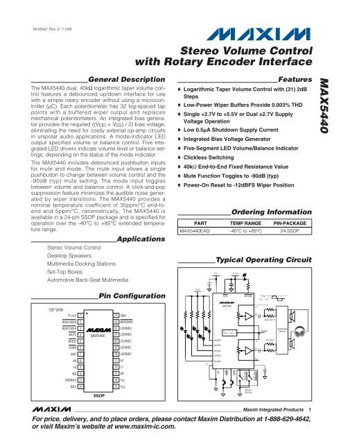
TOP VIEW<br />
VLOGIC 1<br />
RENCODEB 2<br />
RENCODEA 3<br />
MUTE 4<br />
MODE 5<br />
SHDN 6<br />
GND<br />
H0<br />
L0<br />
W0<br />
MIDBIAS<br />
BIAS<br />
8<br />
<strong>MAX5440</strong><br />
17<br />
Stereo Volume Control<br />
with Rotary Encoder Interface<br />
Applications<br />
24 GND<br />
23 MODEIND<br />
22 LEDIND4<br />
21 LEDIND3<br />
20 LEDIND2<br />
19 LEDIND1<br />
7 18 LEDIND0<br />
H1<br />
9 16 L1<br />
10 15 W1<br />
11<br />
12<br />
Pin Configuration<br />
SSOP<br />
14<br />
13<br />
VSS<br />
VDD<br />
Features<br />
♦ Logarithmic Taper Volume Control with (31) 2dB<br />
Steps<br />
♦ Low-Power Wiper Buffers Provide 0.003% THD<br />
♦ Single +2.7V to +5.5V or Dual ±2.7V Supply<br />
Voltage Operation<br />
♦ Low 0.5µA Shutdown Supply Current<br />
♦ Integrated Bias Voltage Generator<br />
♦ Five-Segment LED Volume/Balance Indicator<br />
♦ Clickless Switching<br />
♦ 40kΩ End-to-End Fixed Resistance Value<br />
♦ Mute Function Toggles to -90dB (typ)<br />
♦ Power-On Reset to -12dBFS Wiper Position<br />
________________________________________________________________ <strong>Maxim</strong> Integrated Products 1<br />
VLOGIC<br />
VSS<br />
VDD<br />
LEDIND0<br />
LEDIND1<br />
LEDIND2<br />
LEDIND3<br />
LEDIND4<br />
GND<br />
SHDN<br />
<strong>MAX5440</strong><br />
(VDD + VSS) / 2<br />
MUTE<br />
Ordering Information<br />
PART TEMP RANGE PIN-PACKAGE<br />
<strong>MAX5440</strong>EAG -40°C to +85°C 24 SSOP<br />
Typical Operating Circuit<br />
For price, delivery, and to place orders, please contact <strong>Maxim</strong> Distribution at 1-888-629-4642,<br />
or visit <strong>Maxim</strong>’s website at www.maxim-ic.com.<br />
VLOGIC<br />
MODE<br />
MODEIND<br />
RENCODEA<br />
ROTARY<br />
ENCODER<br />
H1<br />
W1<br />
L1<br />
L0<br />
W0<br />
H0<br />
RENCODEB<br />
VPEAK<br />
(VDD + VSS) / 2<br />
BIAS<br />
MIDBIAS<br />
RIGHT INPUT<br />
LEFT INPUT<br />
HEADPHONE<br />
DRIVER<br />
<strong>MAX5440</strong>
<strong>MAX5440</strong><br />
Stereo Volume Control<br />
with Rotary Encoder Interface<br />
ABSOLUTE MAXIMUM RATINGS<br />
SHDN, MUTE, RENCODEA, RENCODEB,<br />
and MODE to GND............................-0.3V to (VLOGIC + 0.3V)<br />
H_, L_, and W_ to VSS ...............................-0.3V to (VDD + 0.3V)<br />
LEDIND_, MODEIND to GND................-0.3V to (VLOGIC + 0.3V)<br />
MIDBIAS, BIAS to VSS......................(VSS - 0.3V) to (VDD + 0.3V)<br />
VLOGIC to GND...........................................-0.3V to (VDD + 0.3V)<br />
VDD to GND..............................................................-0.3V to +6V<br />
VDD to VSS................................................................-0.3V to +6V<br />
VSS to GND...............................................................-3V to +0.3V<br />
Input and Output Latchup Immunity...............................±200mA<br />
Continuous Power Dissipation (TA = +70°C)<br />
24-Pin SSOP (derate 12.3mW/°C above +70°C) ......987.7mW<br />
Operating Temperature Range ...........................-40°C to +85°C<br />
Junction Temperature......................................................+150°C<br />
Storage Temperature Range .............................-60°C to +150°C<br />
Lead Temperature (soldering, 10s) .................................+300°C<br />
Stresses beyond those listed under “Absolute <strong>Maxim</strong>um Ratings” may cause permanent damage to the device. These are stress ratings only, and functional<br />
operation of the device at these or any other conditions beyond those indicated in the operational sections of the specifications is not implied. Exposure to<br />
absolute maximum rating conditions for extended periods may affect device reliability.<br />
ELECTRICAL CHARACTERISTICS<br />
(VDD = +2.7V to +5.5V, VSS = VGND = 0, 2.7V ≤ (VDD - VSS) ≤ 5.5V, VLOGIC = +2.7V to VDD, VH_ = VDD, VL_ = VDD / 2, TA = TMIN to<br />
TMAX, unless otherwise specified. Typical values are at TA = +25°C.) (Note 1)<br />
PARAMETER SYMBOL CONDITIONS MIN TYP MAX UNITS<br />
End-to-End Resistance R 36 40 52 kΩ<br />
Absolute Tolerance ±0.25 dB<br />
Tap-to-Tap Tolerance ±0.1 dB<br />
Total Harmonic Distortion Plus<br />
Noise<br />
THD+N<br />
V H _= ( V D D / 2) + 1V RM S , 1kH z tap at top , RL<br />
= ∞ to V L_ = V D D / 2, 20H z to 20kH z<br />
V H _= ( V D D / 2) + 1.5V RM S , 1kH z tap at top ,<br />
RL = ∞ to V L_ = V D D / 2, 20H z to 20kH z<br />
VDD = 5V,VSS = 0V, V L_ = 1.5V, VH_ =<br />
(VDD / 2) + 1VRMS, 1kHz tap at top, RL =<br />
10kΩ to VMIDBIAS, 20Hz to 20kHz<br />
VDD = 5V,VSS = 0V, V L_ = 5V, V H _= ( V D D /<br />
2) + 1.5V RM S , 1kHz tap at top, RL = 10kΩ<br />
to VMIDBIAS, 20Hz to 20kHz<br />
Channel Isolation 100 dB<br />
Interchannel Matching ±0.5 dB<br />
Mute Attenuation SHDN = VDD 90 dB<br />
Power-Supply Rejection Ratio PSRR Input referred, 217Hz, 100mVP-P on VDD -60 dB<br />
H Terminal Capacitance CH 5 pF<br />
L Terminal Capacitance CL 7 pF<br />
End-to-End Resistance 35 ppm/°C<br />
Ratiometric Resistance 5 ppm/°C<br />
Bandwidth, -3dB fCUTOFF CW = 33pF 100 kHz<br />
Output Noise en 20Hz to 20kHz 3.2 µVRMS<br />
WIPER BUFFER<br />
Output Voltage Swing VO RL = 10kΩ to VMIDBIAS VDD - 0.2 V<br />
Output Current 3 mA<br />
Output Resistance ROWB 1 10 Ω<br />
DC Offset -14 ±2 +14 mV<br />
INTEGRATED BIAS GENERATOR<br />
Output Voltage ILOAD = 1mA<br />
(VDD +<br />
VSS) / 2<br />
- 30mV<br />
2 _______________________________________________________________________________________<br />
0.004<br />
0.006<br />
0.004<br />
0.006<br />
(VDD +<br />
VSS)<br />
/ 2<br />
( V D D +<br />
V S S ) / 2 +<br />
30m V<br />
%<br />
V
ELECTRICAL CHARACTERISTICS (continued)<br />
Stereo Volume Control<br />
with Rotary Encoder Interface<br />
(VDD = +2.7V to +5.5V, VSS = VGND = 0, 2.7V ≤ (VDD - VSS) ≤ 5.5V, VLOGIC = +2.7V to VDD, VH_ = VDD, VL_ = VDD / 2, TA = TMIN to<br />
TMAX, unless otherwise specified. Typical values are at TA = +25°C.) (Note 1)<br />
PARAMETER SYMBOL CONDITIONS MIN TYP MAX UNITS<br />
Power-Supply Rejection Ratio PSRRBR 1kHz, 100mV on VDD, 1µF on BIAS 60 dB<br />
<strong>Maxim</strong>um Load To VDD or GND 3 kΩ<br />
Output Resistance ROBR 6 Ω<br />
CONTACT INPUTS (MUTE, MODE, RENCODEA, RENCODEB)<br />
Internal Pullup Resistor RPULLUP 45 kΩ<br />
Single Pulse Input Low Time tCPW 22 ms<br />
Repetitive Input Pulse Separation tIPWS 66 ms<br />
Timeout Period tWS Click/pop suppression inactive 32 ms<br />
DIGITAL INPUTS (MUTE, MODE, RENCODEA, RENCODEB, SHDN)<br />
Input High Voltage (Note 2) VIH<br />
Input Low Voltage (Note 2) VIL<br />
3.6V < VLOGIC ≤ 5.5V 2.4<br />
2.7V ≤ VLOGIC ≤ 3.6V 2.0<br />
3.6V < VLOGIC ≤ 5.5V 0.8<br />
2.7V ≤ VLOGIC ≤ 3.6V 0.6<br />
Input Leakage Current Inputs unconnected -1 +1 µA<br />
Input Capacitance 5 pF<br />
POWER SUPPLIES<br />
Supply Voltage VDD VSS = 0 2.7 5.5 V<br />
Negative Power Supply VSS VDD = +2.7V -2.7 0 V<br />
Supply Voltage Difference VDD - VSS 5.5 V<br />
Active Supply Current IDD 1.4 mA<br />
S tand b y S up p l y C ur r ent ( N otes 3, 4) ISTBY<br />
VDD = +5V, VSS = 0 1.3<br />
VDD = +2.7V, VSS = -2.7V 1.3<br />
Shutdown Supply Current ISHDN (Note 3) 1 µA<br />
Power-Up Time tPU Click/pop suppression inactive 50 ms<br />
Logic Supply Voltage VLOGIC VSS = 0 2.7 VDD V<br />
Logic Active Supply Current IL VRENCODEA = VRENCODEB = 0V 320 µA<br />
Logic Standby Supply Current ILSTBY (Note 4) 1 µA<br />
Logic Shutdown Current ILSHDN 1 µA<br />
LED INDICATORS (LEDIND0–LEDIND4, MODEIND)<br />
Output Low Voltage VOL<br />
VLOGIC = 2.7V, ISINK = 10mA 0.4<br />
VLOGIC = 5.5V, ISINK = 10mA 0.2<br />
Output Leakage Current 0.1 10 µA<br />
Output Capacitance 3 pF<br />
<strong>Maxim</strong>um Sink Current 150 mA<br />
Note 1: Parameters are 100% production tested at +85°C and limits through temperature are guaranteed by design.<br />
Note 2: The device draws current in excess of the specified supply current when the digital inputs are driven with voltages between<br />
(VDD - 0.5V) and (GND + 0.5V). See Digital Supply Current vs. Digital Input Voltage in the Typical Operating Characteristics.<br />
Note 3: Shutdown refers to the SHDN input being asserted low. Standby refers to SHDN not being asserted and all I/O inactive.<br />
Note 4: Supply current measured with the wiper position fixed.<br />
_______________________________________________________________________________________ 3<br />
V<br />
V<br />
mA<br />
V<br />
<strong>MAX5440</strong>
<strong>MAX5440</strong><br />
ATTENUATION (dB)<br />
RESPONSE (dB)<br />
Stereo Volume Control<br />
with Rotary Encoder Interface<br />
(TA = +25°C, unless otherwise noted.)<br />
0<br />
-10<br />
-20<br />
-30<br />
-40<br />
-50<br />
-60<br />
-70<br />
-5.2<br />
-5.6<br />
-6.0<br />
-6.4<br />
-6.8<br />
-7.2<br />
-7.6<br />
-8.0<br />
-8.4<br />
-8.8<br />
ATTENUATION vs. TAP POSITION<br />
0 4 8 12 16 20 24 28 32<br />
TAP POSITION<br />
WIPER SWITCHING TRANSIENT<br />
<strong>MAX5440</strong> toc04<br />
51ms<br />
20ms/div<br />
FREQUENCY RESPONSE<br />
VH_ = 2.5 ±1VRMS, VL_ = 2.5V, CL_ = 33pF<br />
W_ SET TO -6dB<br />
0.01 0.1 1 10 100 1000<br />
FREQUENCY (kHz)<br />
<strong>MAX5440</strong> toc01<br />
RENCODEA<br />
RENCODEB<br />
WIPER<br />
TRANSITION<br />
FROM -2dB<br />
TO -4dB<br />
<strong>MAX5440</strong> toc07<br />
END-TO-END RESISTANCE CHANGE (%)<br />
NOMINAL END-TO-END VOLTAGE (%VHL)<br />
THD+N (%)<br />
0.10<br />
0.05<br />
0<br />
-0.05<br />
-0.10<br />
-0.15<br />
-0.20<br />
-0.25<br />
100<br />
90<br />
80<br />
70<br />
60<br />
50<br />
40<br />
30<br />
20<br />
10<br />
0<br />
0.1<br />
0.01<br />
Typical Operating Characteristics<br />
END-TO-END RESISTANCE % CHANGE<br />
vs. TEMPERATURE<br />
-40 -15 10 35 60 85<br />
TEMPERATURE (°C)<br />
WIPER-TO-END TERMINAL VOLTAGE<br />
vs. TAP POSITION<br />
0 4 8 12 16 20 24 28 32<br />
TAP POSITION<br />
4 _______________________________________________________________________________________<br />
VHW<br />
VWL<br />
THD+N vs. FREQUENCY<br />
VDD = 2.5V<br />
VSS = -2.5V<br />
L_ = VMIDBIAS<br />
H_ = VMIDBIAS + 1VRMS<br />
W_ SET AT -2dB<br />
W_ SET AT 0dB<br />
0.001<br />
0.001 0.01 0.1 1 10 100<br />
FREQUENCY (kHz)<br />
W_ SET AT -6dB<br />
<strong>MAX5440</strong> toc02<br />
<strong>MAX5440</strong> toc05<br />
<strong>MAX5440</strong> toc08<br />
TOTAL SUPPLY CURRENT (mA)<br />
RESPONSE (dB)<br />
THD+N (%)<br />
1.48<br />
1.47<br />
1.46<br />
1.45<br />
1.44<br />
1.43<br />
1.42<br />
1.41<br />
1.40<br />
1.39<br />
1.38<br />
0.8<br />
0.4<br />
0<br />
-0.4<br />
-0.8<br />
-1.2<br />
-1.6<br />
-2.0<br />
-2.4<br />
-2.8<br />
0.1<br />
0.01<br />
TOTAL SUPPLY CURRENT<br />
vs. TEMPERATURE<br />
VLOGIC = VDD = 5.5V<br />
-40 -15 10 35 60 85<br />
TEMPERATURE (°C)<br />
FREQUENCY RESPONSE<br />
VH_ = 2.5 ±1VRMS, VL_ = 2.5V, CL_ = 33pF<br />
W_ SET TO 0dB<br />
0.01 0.1 1 10 100 1000<br />
FREQUENCY (kHz)<br />
THD+N vs. FREQUENCY<br />
VDD = 5.0V<br />
VSS = GND<br />
L_ = VMIDBIAS<br />
H_ = VMIDBIAS + 1VRMS<br />
W_ SET AT -2dB<br />
0.001<br />
0.001 0.01 0.1 1 10 100<br />
FREQUENCY (kHz)<br />
W_ SET AT -6dB<br />
W_ SET AT 0dB<br />
<strong>MAX5440</strong> toc03<br />
<strong>MAX5440</strong> toc06<br />
<strong>MAX5440</strong> toc09
(VDD = +5V, TA = +25°C, unless otherwise noted.)<br />
RESPONSE (dB)<br />
-25<br />
-30<br />
-35<br />
-40<br />
-45<br />
-50<br />
-55<br />
-60<br />
-65<br />
-70<br />
-75<br />
POWER-SUPPLY REJECTION RATIO<br />
vs. FREQUENCY<br />
VDD_ = 5V ±100mVP-P, VH = 5V<br />
VL_ = 2.5V, W_ SET TO -6dB<br />
0.01 0.1 1<br />
FREQUENCY (kHz)<br />
10 100<br />
SUPPLY CURRENT (mA)<br />
1.1768<br />
1.1766<br />
1.1764<br />
1.1762<br />
1.1760<br />
1.1758<br />
1.1756<br />
1.1754<br />
NOISE (nV/√Hz)<br />
1.1770<br />
1.1752<br />
1200<br />
1000<br />
800<br />
600<br />
400<br />
200<br />
0<br />
<strong>MAX5440</strong> toc10<br />
LOGIC SUPPLY CURRENT (µA)<br />
Stereo Volume Control<br />
with Rotary Encoder Interface<br />
300<br />
250<br />
200<br />
150<br />
100<br />
50<br />
ACTIVE SUPPLY CURRENT<br />
vs. TEMPERATURE<br />
VDD = VLOGIC = 5.5V,<br />
RENCODEA = RENCODEB = 0<br />
LOGIC SUPPLY CURRENT<br />
vs. LOGIC SUPPLY VOLTAGE<br />
ACTIVE CURRENT<br />
SHUTDOWN<br />
-40 -15 10 35 60 85<br />
TEMPERATURE (°C)<br />
SPECTRAL NOISE DENSITY<br />
0.01 0.1 1 10 100<br />
FREQUENCY (kHz)<br />
Typical Operating Characteristics (continued)<br />
STANDBY CURRENT<br />
0<br />
2.5 3.0 3.5 4.0 4.5 5.0 5.5<br />
LOGIC SUPPLY VOLTAGE (V)<br />
<strong>MAX5440</strong> toc13<br />
<strong>MAX5440</strong> toc15<br />
DIGITAL SUPPLY CURRENT (µA)<br />
SUPPLY CURRENT (mA)<br />
1000<br />
100<br />
10<br />
8<br />
7<br />
6<br />
5<br />
4<br />
3<br />
2<br />
1<br />
<strong>MAX5440</strong> toc11<br />
LOGIC SUPPLY CURRENT (µA)<br />
350<br />
300<br />
250<br />
200<br />
150<br />
100<br />
50<br />
DIGITAL SUPPLY CURRENT<br />
vs. DIGITAL INPUT VOLTAGE<br />
0<br />
ACTIVE LOGIC SUPPLY CURRENT<br />
vs. TEMPERATURE<br />
VDD = VLOGIC = 5.5V,<br />
RENCODEA = RENCODEB = 0<br />
0 0.5 1.0 1.5 2.0 2.5 3.0 3.5 4.0 4.5 5.0<br />
DIGITAL INPUT VOLTAGE (V)<br />
SUPPLY CURRENT<br />
vs. INPUT VOLTAGE SWEEP<br />
VDD = VLOGIC = 5V, W_ AT 0dB<br />
RL = 10kΩ TO VMIDBIAS<br />
0<br />
2.5 3.0 3.5 4.0 4.5 5.0<br />
INPUT VOLTAGE SWEEP (VH_)<br />
-40 -15 10 35 60 85<br />
TEMPERATURE (°C)<br />
_______________________________________________________________________________________ 5<br />
<strong>MAX5440</strong> toc14<br />
<strong>MAX5440</strong> toc16<br />
<strong>MAX5440</strong> toc12<br />
<strong>MAX5440</strong>
<strong>MAX5440</strong><br />
Stereo Volume Control<br />
with Rotary Encoder Interface<br />
PIN NAME FUNCTION<br />
1 VLOGIC<br />
2 RENCODEB<br />
3 RENCODEA<br />
4 MUTE<br />
5 MODE<br />
6 SHDN<br />
Digital Logic Power Supply. Bypass VLOGIC to ground with a 0.1µF capacitor as close to the device<br />
as possible.<br />
Rotary Encoder Input B. With RENCODEA, this input provides the rotary encoder control for the<br />
potentiometer (see Figure 1). RENCODEB is internally pulled up to VLOGIC with a 45kΩ resistor.<br />
Rotary Encoder Input A. With RENCODEB, this input provides the rotary encoder control for the<br />
potentiometer (see Figure 1). RENCODEA is internally pulled up to VLOGIC with a 45kΩ resistor.<br />
Mute Input. Pull MUTE low to toggle the wiper between the mute setting (see Table 1) and the current<br />
setting. MUTE is pulled up to VLOGIC with an internal 45kΩ resistor.<br />
Volume/Balance Control Input. Each high-to-low transition on MODE toggles between the volume and<br />
balance modes. MODE is pulled high internally with a 45kΩ resistor to VLOGIC. On power-up, the<br />
<strong>MAX5440</strong> is in volume-control mode.<br />
Active-Low Shutdown Input. Drive SHDN low to place the device in shutdown mode. In shutdown<br />
mode, the <strong>MAX5440</strong> stores the last wipers settings. The wipers move to the L_ end of the resistor<br />
string. Terminating shutdown mode restores the wipers to their previous settings.<br />
7, 24 GND Ground. Connect pins 7 and 24 together.<br />
8 H0 Potentiometer 0 High Terminal. H0 and L0 terminals can be reversed.<br />
9 L0 Potentiometer 0 Low Terminal. L0 and H0 terminals can be reversed.<br />
10 W0 Potentiometer 0 Wiper Buffered Output<br />
11 MIDBIAS Midbias Voltage Output. VMIDBIAS = (VDD + VSS) / 2.<br />
12 BIAS Bias Generator Input. Bypass with a 1µF capacitor to system ground.<br />
13 VDD<br />
Analog Power Supply. Bypass VDD to ground with a 0.1µF capacitor as close to the device as<br />
possible.<br />
14 VSS<br />
Negative Power Supply. Bypass VSS to ground with a 0.1µF capacitor as close to the device as<br />
possible. Connect to GND for single-supply operation.<br />
15 W1 Potentiometer 1 Wiper Buffered Output<br />
16 L1 Potentiometer 1 Low Terminal. L1 and H1 terminals can be reversed.<br />
17 H1 Potentiometer 1 High Terminal. H1 and L1 terminals can be reversed.<br />
18–22<br />
LEDIND0–<br />
LEDIND4<br />
23 MODEIND<br />
LE D Ind i cator O p en- D r ai n Outp ut 0 thr oug h LE D Ind i cator O p en- D r ai n Outp ut 4. LE D IN D 0–LE D IN D 4 for m a<br />
b ar g r ap h i nd i cati on of the cur r ent vol um e or b al ance. In vol um e m od e, al l LE D s off i nd i cates m ute and al l<br />
LE D s on i nd i cates m axi m um vol um e. In b al anced m od e, LE D 2 on i nd i cates center ed or b al anced .<br />
Volume-Control/Balance-Control Mode Indicator Open-Drain Output. Connect to an LED through a<br />
resistor to VLOGIC. When the LED is on, the <strong>MAX5440</strong> is in balance-control mode. When the LED is<br />
off, the <strong>MAX5440</strong> is in volume-control mode.<br />
6 _______________________________________________________________________________________<br />
Pin Description
Detailed Description<br />
The <strong>MAX5440</strong> dual, 40kΩ logarithmic taper digital<br />
potentiometer features a debounced up/down interface<br />
for use with a simple rotary encoder without using a<br />
microcontroller. Each potentiometer has 32 log-spaced<br />
tap points with a buffered wiper output and replaces<br />
mechanical potentiometers.<br />
Mode Control (MODE)<br />
The <strong>MAX5440</strong> MODE input toggles between volume<br />
and balance modes. Force MODE low to toggle<br />
between volume and balance modes. For example, driving<br />
MODE low once while in volume-control mode<br />
switches the <strong>MAX5440</strong> to balance mode. Driving MODE<br />
low again switches the <strong>MAX5440</strong> back to volume mode.<br />
MODE is internally pulled high with a 45kΩ resistor to<br />
VLOGIC. The <strong>MAX5440</strong> powers up in volume-control<br />
mode. Leave unconnected or connect to VLOGIC if balance<br />
mode is not required.<br />
ROTARY<br />
ENCODER<br />
RENCODEA<br />
RENCODEB<br />
Figure 1. Rotary Encoder Interface<br />
VLOGIC<br />
45kΩ 45kΩ<br />
<strong>MAX5440</strong><br />
A<br />
B<br />
GND<br />
CLOCKWISE ROTATION<br />
INCREASING GRAY CODE (AB) 11, 10, 00, 01, 11, 10, ETC.<br />
COUNTERCLOCKWISE ROTATION<br />
DECREASING GRAY CODE (AB) 11, 01, 00, 10, 11, 01, ETC.<br />
Stereo Volume Control<br />
with Rotary Encoder Interface<br />
1/4 CYCLE PER DETENT<br />
CW<br />
OPEN CIRCUIT<br />
CLOSED CIRCUIT<br />
OPEN CIRCUIT<br />
CLOSED CIRCUIT<br />
Rotary Encoder Interface<br />
The <strong>MAX5440</strong> interfaces with rotary encoder switches.<br />
The rotary encoder is a contact closure type switch with<br />
two outputs that connect to RENCODEA and<br />
RENCODEB on the device. As the shaft is rotated,<br />
RENCODEA and RENCODEB produce a gray code<br />
count. Figure 1 shows a typical rotary encoder interface.<br />
State changes trigger a wiper movement and the direction<br />
of the count dictates the direction of wiper movement.<br />
An increasing gray code count moves the wiper<br />
up to a lower attenuation setting in volume mode and<br />
towards a full right channel (CH1) in balance mode. A<br />
decreasing gray code count moves the wiper down to a<br />
higher attenuation in volume mode and towards a full left<br />
channel (CH0) in balance mode. Both switch inputs are<br />
internally pulled up to VLOGIC by internal 45kΩ resistors.<br />
During rapid rotation, the inputs must be stable for at<br />
least 20ms and have separation between state<br />
changes by at least 40ms for the debounce circuitry to<br />
accurately detect the input states.<br />
CHANNEL A<br />
D D D D D D D D D D D D D D D D D<br />
CHANNEL B<br />
_______________________________________________________________________________________ 7<br />
<strong>MAX5440</strong>
<strong>MAX5440</strong><br />
Stereo Volume Control<br />
with Rotary Encoder Interface<br />
Volume Control<br />
In volume-control mode, the <strong>MAX5440</strong>’s wipers move<br />
simultaneously, maintaining the balance separation<br />
between each wiper (Figure 2a).<br />
When either wiper reaches the maximum tap position<br />
(position closest to H_), further commands to increase<br />
the volume are ignored. Balance separation is maintained<br />
in the maximum volume configuration (Figure 2b).<br />
When either wiper reaches the minimum tap position<br />
(position closest to L_), further commands to decrease<br />
FROM C<br />
H_<br />
L_<br />
H_<br />
L_<br />
H_<br />
L_<br />
H_<br />
L_<br />
Figure 2. Volume-Control Operation<br />
W0<br />
W1 W0<br />
ROTATE CW<br />
TWICE<br />
ROTATE CCW<br />
ONCE<br />
BALANCE SEPARATION<br />
MAINTAINED<br />
NO CHANGE<br />
W0 W1 W0 W1 W0 W1<br />
ROTATE CW<br />
ONCE<br />
ROTATE CCW<br />
ONCE<br />
ROTATE CW<br />
ROTATE CCW<br />
ORIGINAL BALANCE SEPARATION<br />
MAINTAINED<br />
W0 W1 W0 W1 W0 W1<br />
ROTATE CW<br />
ONCE<br />
the volume adjust the other wiper until it also reaches<br />
the minimum tap position (Figure 2c).<br />
Increasing the volume from this minimum position<br />
restores the original balance separation of the wipers<br />
(Figure 2d).<br />
When both wipers are in the tap 31 position (-62dB<br />
attenuation), further decreasing rotations place the<br />
wipers in the mute position (see Table 1). Rotating the<br />
encoder to a lower attenuation or a pulse to MUTE<br />
returns the wipers to tap 31.<br />
W1 W0 W1<br />
W0 W1 W0 W1 W0 W1<br />
ROTATE CW<br />
ONCE<br />
8 _______________________________________________________________________________________<br />
a<br />
b<br />
c<br />
d<br />
TO D
Table 1. Wiper Position and Attenuation<br />
POSITION ATTENUATION (dB)<br />
0 0<br />
1 -2<br />
2 -4<br />
… …<br />
6 (POR) -12<br />
… …<br />
30 -60<br />
31 -62<br />
32 (MUTE) ≥ 90<br />
H_<br />
L_<br />
H_<br />
L_<br />
VOLUME LEVEL IS SET<br />
Stereo Volume Control<br />
with Rotary Encoder Interface<br />
Balance Control<br />
In balance-control mode, the <strong>MAX5440</strong> adjusts the balance<br />
between channel 0 and channel 1 while maintaining<br />
the set volume. For example, if the volume of<br />
channel 0 equals the volume of channel 1, forcing the<br />
balance towards channel 1 increases the attenuation of<br />
channel 0 (Figure 3a). If channel 1 is at a higher attenuation<br />
than channel 0, adjusting the balance to channel<br />
1 moves channel 1’s wiper up to the same wiper position<br />
as channel 0 before it was attenuated (Figure 3b).<br />
Click-and-Pop Suppression<br />
The click-and-pop suppression feature reduces the<br />
audible noise (clicks and pops) that results from wiper<br />
transitions. The <strong>MAX5440</strong> minimizes this noise by allowing<br />
the wiper to change position only when VH = VL.<br />
Each wiper has its own suppression and timeout circuitry.<br />
The <strong>MAX5440</strong> changes wiper position when VH<br />
= VL, or after 32ms, whichever occurs first (see Figures<br />
4a and 4b).<br />
The suppression circuitry monitors left and right channels<br />
separately. In volume-control mode, when the first<br />
wiper changes position, the second wiper has 32ms to<br />
change or it will be forced to change.<br />
W0 W1 W0 W1 W0 W1<br />
VOLUME LEVEL IS SET BY W0<br />
Figure 3. Balance-Control Operation<br />
ROTATE CW<br />
ONCE<br />
ROTATE CW<br />
ONCE<br />
W0 W1 W0 W1 W0 W1<br />
ROTATE CW<br />
ONCE<br />
ROTATE CW<br />
ONCE<br />
VOLUME LEVEL MAINTAINED<br />
BALANCE SHIFTS TO W1<br />
VOLUME LEVEL MAINTAINED<br />
BALANCE SHIFTS TO W1<br />
_______________________________________________________________________________________ 9<br />
<strong>MAX5440</strong>
<strong>MAX5440</strong><br />
Stereo Volume Control<br />
with Rotary Encoder Interface<br />
USER ROTATES ENCODER<br />
01<br />
00<br />
VH_<br />
VL_<br />
WIPER MOTION<br />
SWITCH<br />
CONTACT<br />
IS BOUNCING<br />
SWITCH<br />
CONTACT<br />
IS STABLE<br />
tLPW<br />
DEBOUNCE BY WAITING<br />
FOR STABLE LOW, tLPW<br />
INPUT ACCEPTED<br />
10 ______________________________________________________________________________________<br />
tWS<br />
WAIT FOR FIRST<br />
ZERO CROSSING, tWS<br />
Figure 4a. Wiper Transition Timing Diagram—Suppression Circuitry Active<br />
WIPER MOVES HERE<br />
SWITCH CONTACT<br />
IS BOUNCING<br />
2dB STEPS<br />
tHPW<br />
DEBOUNCE BY WAITING<br />
FOR STABLE HIGH, tHPW
01<br />
00<br />
VH<br />
VL<br />
SWITCH CONTACT<br />
IS BOUNCING<br />
tLPW<br />
SWITCH<br />
CONTACT<br />
IS STABLE<br />
DEBOUNCE BY WAITING<br />
FOR STABLE LOW, tLPW<br />
Stereo Volume Control<br />
with Rotary Encoder Interface<br />
(tLPW + tWS)<br />
Figure 4b. Wiper Transition Timing Diagram—Timed Out<br />
INPUT ACCEPTED<br />
tWS<br />
WAIT FOR FIRST<br />
ZERO CROSSING OR<br />
TIMEOUT, tWS<br />
WIPER MOVES HERE<br />
SWITCH CONTACT<br />
IS BOUNCING<br />
2dB STEPS<br />
tHPW<br />
DEBOUNCE BY WAITING<br />
FOR STABLE HIGH, tHPW<br />
READY TO ACCEPT ANOTHER<br />
ENCODER INPUT SIGNAL<br />
______________________________________________________________________________________ 11<br />
<strong>MAX5440</strong>
<strong>MAX5440</strong><br />
Stereo Volume Control<br />
with Rotary Encoder Interface<br />
Power-On Reset<br />
The power-on comparators monitor (VDD - VSS) and<br />
(VLOGIC - GND). A power-on reset is initiated when<br />
either of the supplies is brought back to the normal<br />
operating voltage. The power-on reset feature sets both<br />
wipers to -12dB. The wipers initially wake up in mute<br />
mode (-90dB) and move to the -12dB position when VH<br />
= VL to eliminate clicks and pops during power-up.<br />
With DC inputs at VH and VL, the wipers move after<br />
exceeding the timeout period. A power-on reset places<br />
the <strong>MAX5440</strong> in volume-control mode.<br />
Shutdown (SHDN)<br />
Upon entering shutdown, the <strong>MAX5440</strong> stores the last<br />
wiper settings. The wipers move to the L_ end of the<br />
resistor string. The wipers move to the L_ end of the<br />
resistor string when VH = VL to eliminate clicks and pops<br />
during shutdown. With DC inputs at VH and VL, the<br />
wipers move after exceeding the timeout period. Exiting<br />
shutdown restores the wipers to their previous settings.<br />
Mute Function (MUTE)<br />
The <strong>MAX5440</strong> features a mute function input, MUTE.<br />
Successive low pulses on MUTE toggle its setting.<br />
Activating the mute function forces both wipers to maximum<br />
attenuation (-90dB typ). Deactivating the mute<br />
function returns the wipers to their previous settings.<br />
Rotating the encoder clockwise (increasing gray code<br />
count) also deactivates mute, setting the wipers to their<br />
previous positions. MUTE is internally pulled high with a<br />
45kΩ resistor to VLOGIC. When both wipers are in the<br />
tap 31 position (-62dB attenuation) further commands<br />
to lower the volume (decreasing gray code count)<br />
place the wipers in the mute position (see Table 1).<br />
Rotating the encoder to a lower attenuation or a pulse<br />
to MUTE returns the wipers to tap 31.<br />
Table 2. LED Settings in Volume Mode<br />
VOLUME POSITION (dB)<br />
Mode Indicator (MODEIND)<br />
The open-drain MODEIND indicates volume-control<br />
mode or balance-control mode for the <strong>MAX5440</strong>.<br />
Connect MODEIND to an LED with a series resistor to<br />
VLOGIC. When the LED is on, the <strong>MAX5440</strong> is in balancecontrol<br />
mode. When the LED is off, the <strong>MAX5440</strong> is in<br />
volume-control mode. See the Mode Control (MODE)<br />
section for more detail on switching between modes.<br />
Level Indicator LEDs<br />
The <strong>MAX5440</strong> includes five indicator LED drivers to display<br />
the current wiper settings in either volume or balance<br />
mode. Connect the LEDIND_ outputs to the LEDs<br />
and to VLOGIC through a series resistor as shown in the<br />
typical application circuits.<br />
In volume-control mode, all LEDs are off when the<br />
wipers reach the highest attenuation levels (mute). All<br />
LEDs are on at the lowest attenuation levels (0dB).<br />
Table 2 shows the LED display as the wipers transition<br />
through various attenuation levels.<br />
In balance-control mode, only one LED is on at a time<br />
to indicate the current balance setting. Figure 5 shows<br />
the LEDs display for the current balance setting. When<br />
LED2 is on, the display indicates that the channels are<br />
centered or balanced at a set volume level. Turning the<br />
encoder clockwise (an increasing gray code count)<br />
turns LED3 on to represent a balance shift towards<br />
channel 1. When LED4 turns on, the balance shifts<br />
completely toward channel 1 and channel 0 is fully<br />
attenuated. From a balanced position, turning the<br />
encoder counterclockwise (a decreasing gray code<br />
count) turns on LED1, and then LED0 to indicate a balance<br />
shift towards channel 0.<br />
VOLUME LED OUTPUTS (1 = LED IS ON)<br />
LED0 LED1 LED2 LED3 LED4<br />
0 to -8 1 1 1 1 1<br />
-10 to -18 1 1 1 1 0<br />
-20 to -28 1 1 1 0 0<br />
-30 to -38 1 1 0 0 0<br />
-40 to -52 1 0 0 0 0<br />
-54 to mute (-90) 0 0 0 0 0<br />
12 ______________________________________________________________________________________
Stereo Volume Control<br />
with Rotary Encoder Interface<br />
FULL L L + 12 L + 6 R + 6 R + 12 FULL R<br />
CCW ROTATION (CH0)<br />
CENTERED CW ROTATION (CH1)<br />
LED0 ON LED1 ON LED2 ON LED3 ON LED4 ON<br />
Figure 5. LED Setting in Balance Mode<br />
VLOGIC<br />
VSS = -VDD<br />
VDD<br />
LEDIND0<br />
LEDIND1<br />
LEDIND2<br />
LEDIND3<br />
LEDIND4<br />
Figure 6. Dual-Supply Volume/Balance Control<br />
GND<br />
SHDN<br />
<strong>MAX5440</strong><br />
(VDD + VSS) / 2<br />
MUTE<br />
VLOGIC<br />
MODE<br />
MODEIND<br />
MIDBIAS<br />
RENCODEA<br />
ROTARY<br />
ENCODER<br />
H1<br />
W1<br />
L1<br />
L0<br />
W0<br />
H0<br />
RENCODEB<br />
BIAS<br />
VPEAK<br />
0V<br />
RIGHT INPUT<br />
LEFT INPUT<br />
HEADPHONE<br />
DRIVER<br />
______________________________________________________________________________________ 13<br />
<strong>MAX5440</strong>
<strong>MAX5440</strong><br />
Stereo Volume Control<br />
with Rotary Encoder Interface<br />
Multiple Button Pushes (MODE, MUTE)<br />
The <strong>MAX5440</strong> does not respond to simultaneous button<br />
pushes. Pushing more than one button at the same<br />
time stops the wipers in their present states. Only a single<br />
button push configures the device.<br />
Applications Information<br />
Typical Application Circuit<br />
The Typical Operating Circuit shows the <strong>MAX5440</strong> in a<br />
typical volume/balance application using a single-supply<br />
configuration. Figure 6 shows a typical volume/balance<br />
application circuit using the <strong>MAX5440</strong> in a<br />
dual-supply configuration. The <strong>MAX5440</strong> does not<br />
require external op amps because the bias is generated<br />
internally, and the wipers have internal low-power<br />
buffers for low distortion. Connect the W_ outputs of the<br />
<strong>MAX5440</strong> to the left and right inputs of a stereo audio<br />
amplifier, such as the MAX9761. The rotary encoder<br />
controls the potentiometer attenuation levels without<br />
using a microcontroller. Use the MODE input to switch<br />
between volume-control and balance-control modes.<br />
PROCESS: BiCMOS<br />
14 ______________________________________________________________________________________<br />
Chip Information
H0<br />
W0<br />
L0<br />
VLOGIC<br />
0<br />
1<br />
2<br />
3<br />
4<br />
28<br />
29<br />
30<br />
31<br />
<strong>MAX5440</strong><br />
SHDN<br />
MODEIND<br />
Stereo Volume Control<br />
with Rotary Encoder Interface<br />
CLICK-AND-POP<br />
SUPPRESSION<br />
CIRCUITRY<br />
POSITION COUNTER POSITION COUNTER<br />
UP/DOWN UP/DOWN<br />
TIMING AND CONTROL<br />
DEBOUNCE DEBOUNCE DEBOUNCE DEBOUNCE DEBOUNCE<br />
GND RENCODEA RENCODEB MODE<br />
MUTE<br />
VDD<br />
VSS<br />
VLOGIC<br />
Functional Diagram<br />
MUTE MUTE<br />
Package Information<br />
For the latest package outline information and land patterns, go<br />
to www.maxim-ic.com/packages.<br />
PACKAGE TYPE PACKAGE CODE DOCUMENT NO.<br />
24 SSOP A24-1 21-0056<br />
BIAS<br />
BIAS GENERATOR<br />
45kΩ 45kΩ 45kΩ 45kΩ<br />
MIDBIAS<br />
CLICK-AND-POP<br />
SUPPRESSION<br />
CIRCUITRY<br />
______________________________________________________________________________________ 15<br />
LEDIND0<br />
LEDIND1<br />
LEDIND2<br />
LEDIND3<br />
LEDIND4<br />
0<br />
1<br />
2<br />
3<br />
4<br />
28<br />
29<br />
30<br />
31<br />
H1<br />
W1<br />
L1<br />
<strong>MAX5440</strong>
<strong>MAX5440</strong><br />
Stereo Volume Control<br />
with Rotary Encoder Interface<br />
REVISION<br />
NUMBER<br />
REVISION<br />
DATE<br />
DESCRIPTION<br />
Revision History<br />
PAGES<br />
CHANGED<br />
2 11/08 Fixed pin names and thermal data. Updated two specifications in EC table 1, 2, 3, 6, 13<br />
<strong>Maxim</strong> cannot assume responsibility for use of any circuitry other than circuitry entirely embodied in a <strong>Maxim</strong> product. No circuit patent licenses are<br />
implied. <strong>Maxim</strong> reserves the right to change the circuitry and specifications without notice at any time.<br />
16 ____________________<strong>Maxim</strong> Integrated Products, 120 San Gabriel Drive, Sunnyvale, CA 94086 408-737-7600<br />
© 2008 <strong>Maxim</strong> Integrated Products is a registered trademark of <strong>Maxim</strong> Integrated Products, Inc.