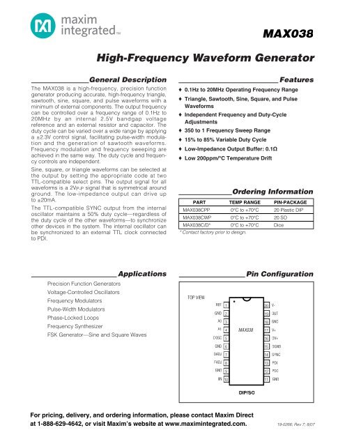
MAX038: High-Frequency Waveform Generator - Maxim
MAX038: High-Frequency Waveform Generator - Maxim
MAX038: High-Frequency Waveform Generator - Maxim

You also want an ePaper? Increase the reach of your titles
YUMPU automatically turns print PDFs into web optimized ePapers that Google loves.
AVAILABLE<br />
General Description<br />
The <strong>MAX038</strong> is a high-frequency, precision function<br />
generator producing accurate, high-frequency triangle,<br />
sawtooth, sine, square, and pulse waveforms with a<br />
minimum of external components. The output frequency<br />
can be controlled over a frequency range of 0.1Hz to<br />
20MHz by an internal 2.5V bandgap voltage<br />
reference and an external resistor and capacitor. The<br />
duty cycle can be varied over a wide range by applying<br />
a ±2.3V control signal, facilitating pulse-width modulation<br />
and the generation of sawtooth waveforms.<br />
<strong>Frequency</strong> modulation and frequency sweeping are<br />
achieved in the same way. The duty cycle and frequency<br />
controls are independent.<br />
Sine, square, or triangle waveforms can be selected at<br />
the output by setting the appropriate code at two<br />
TTL-compatible select pins. The output signal for all<br />
waveforms is a 2VP-P signal that is symmetrical around<br />
ground. The low-impedance output can drive up<br />
to ±20mA.<br />
The TTL-compatible SYNC output from the internal<br />
oscillator maintains a 50% duty cycle—regardless of<br />
the duty cycle of the other waveforms—to synchronize<br />
other devices in the system. The internal oscillator can<br />
be synchronized to an external TTL clock connected<br />
to PDI.<br />
Functional Diagrams<br />
Applications<br />
Precision Function <strong>Generator</strong>s<br />
Voltage-Controlled Oscillators<br />
<strong>Frequency</strong> Modulators<br />
Pulse-Width Modulators<br />
Phase-Locked Loops<br />
<strong>Frequency</strong> Synthesizer<br />
FSK <strong>Generator</strong>—Sine and Square Waves<br />
Pin Configurations appear at end of data sheet.<br />
Functional Diagrams continued at end of data sheet.<br />
UCSP is a trademark of <strong>Maxim</strong> Integrated Products, Inc.<br />
<strong>High</strong>-<strong>Frequency</strong> <strong>Waveform</strong> <strong>Generator</strong><br />
For pricing, delivery, and ordering information, please contact <strong>Maxim</strong> Direct<br />
at 1-888-629-4642, or visit <strong>Maxim</strong>’s website at www.maximintegrated.com.<br />
Features<br />
♦ 0.1Hz to 20MHz Operating <strong>Frequency</strong> Range<br />
♦ Triangle, Sawtooth, Sine, Square, and Pulse<br />
<strong>Waveform</strong>s<br />
♦ Independent <strong>Frequency</strong> and Duty-Cycle<br />
Adjustments<br />
♦ 350 to 1 <strong>Frequency</strong> Sweep Range<br />
♦ 15% to 85% Variable Duty Cycle<br />
♦ Low-Impedance Output Buffer: 0.1Ω<br />
♦ Low 200ppm/°C Temperature Drift<br />
TOP VIEW<br />
REF 1<br />
GND 2<br />
A0 3<br />
A1 4<br />
COSC 5<br />
GND 6<br />
DADJ 7<br />
FADJ 8<br />
GND 9<br />
IIN 10<br />
Ordering Information<br />
PART TEMP RANGE PIN-PACKAGE<br />
<strong>MAX038</strong>CPP 0°C to +70°C 20 Plastic DIP<br />
<strong>MAX038</strong>CWP 0°C to +70°C 20 SO<br />
<strong>MAX038</strong>C/D* 0°C to +70°C Dice<br />
* Contact factory prior to design.<br />
<strong>MAX038</strong><br />
DIP/SO<br />
<strong>MAX038</strong><br />
Pin Configuration<br />
20<br />
19<br />
18<br />
17<br />
16<br />
15<br />
14<br />
13<br />
12<br />
11<br />
V-<br />
OUT<br />
GND<br />
V+<br />
DV+<br />
DGND<br />
SYNC<br />
PDI<br />
PDO<br />
GND<br />
19-0266; Rev 7; 8/07
<strong>MAX038</strong><br />
<strong>High</strong>-<strong>Frequency</strong> <strong>Waveform</strong> <strong>Generator</strong><br />
ABSOLUTE MAXIMUM RATINGS<br />
V+ to GND ...............................................................-0.3V to +6V<br />
DV+ to DGND...........................................................-0.3V to +6V<br />
V- to GND .................................................................+0.3V to -6V<br />
Pin Voltages<br />
IIN, FADJ, DADJ, PDO .....................(V- - 0.3V) to (V+ + 0.3V)<br />
COSC ......................................................................+0.3V to V<br />
A0, A1, PDI, SYNC, REF.............................................-0.3V to V+<br />
GND to DGND ...................................................................±0.3V<br />
<strong>Maxim</strong>um Current into Any Pin ........................................±50mA<br />
OUT, REF Short-Circuit Duration to GND, V+, V- ..................30s<br />
Stresses beyond those listed under “Absolute <strong>Maxim</strong>um Ratings” may cause permanent damage to the device. These are stress ratings only, and functional<br />
operation of the device at these or any other conditions beyond those indicated in the operational sections of the specifications is not implied. Exposure to<br />
absolute maximum rating conditions for extended periods may affect device reliability.<br />
ELECTRICAL CHARACTERISTICS<br />
Continuous Power Dissipation (TA = +70°C)<br />
Plastic DIP (derate 11.11mW/°C above +70°C) .........889mW<br />
SO (derate 10.00mW/°C above +70°C).......................800mW<br />
CERDIP (derate 11.11mW/°C above +70°C)...............889mW<br />
Operating Temperature Ranges<br />
<strong>MAX038</strong>C_ _ ......................................................0°C to +70°C<br />
<strong>Maxim</strong>um Junction Temperature . ...................................+150°C<br />
Storage Temperature Range ............................-65°C to +150°C<br />
Lead Temperature (soldering, 10s) .................................+300°C<br />
(Circuit of Figure 1, GND = DGND = 0V, V+ = DV+ = 5V, V- = -5V, VDADJ = VFADJ = VPDI = VPDO = 0V, CF = 100pF,<br />
RIN = 25kΩ RL = 1kΩ, CL = 20pF, TA = TMIN to TMAX, unless otherwise noted. Typical values are at TA = +25°C.)<br />
PARAMETER SYMBOL CONDITIONS MIN TYP MAX UNITS<br />
FREQUENCY CHARACTERISTICS<br />
<strong>Maxim</strong>um Operating <strong>Frequency</strong> Fo CF ≤ 15pF, IIN = 500µA 20.0 40.0 MHz<br />
<strong>Frequency</strong> Programming<br />
Current<br />
IIN<br />
VFADJ = 0V<br />
VFADJ = -3V<br />
2.50<br />
1.25<br />
750<br />
375<br />
µA<br />
IIN Offset Voltage VIN ±1.0 ±2.0 mV<br />
<strong>Frequency</strong> Temperature<br />
Coefficient<br />
ΔFo/°C<br />
Fo/°C<br />
VFADJ = 0V<br />
VFADJ = -3V<br />
600<br />
200<br />
ppm/°C<br />
<strong>Frequency</strong> Power-Supply<br />
Rejection<br />
(ΔFo/Fo)<br />
ΔV+<br />
(ΔFo/Fo)<br />
ΔV-<br />
V- = -5V, V+ = 4.75V to 5.25V<br />
V+ = 5V, V- = -4.75V to -5.25V<br />
±0.4<br />
±0.2<br />
±2.00<br />
±1.00<br />
%/V<br />
OUTPUT AMPLIFIER (applies to all waveforms)<br />
Output Peak-to-Peak Symmetry VOUT ±4 mV<br />
Output Resistance ROUT 0.1 0.2 Ω<br />
Output Short-Circuit Current IOUT Short circuit to GND 40 mA<br />
SQUARE-WAVE OUTPUT (RL = 100Ω)<br />
Amplitude VOUT 1.9 2.0 2.1 VP-P<br />
Rise Time tR 10% to 90% 12 ns<br />
Fall Time tF 90% to 10% 12 ns<br />
Duty Cycle dc VDADJ = 0V, dc = tON/t x 100% 47 50 53 %<br />
TRIANGLE-WAVE OUTPUT (RL = 100Ω)<br />
Amplitude VOUT 1.9 2.0 2.1 VP-P<br />
Nonlinearity FO = 100kHz, 5% to 95% 0.5 %<br />
Duty Cycle<br />
SINE-WAVE OUTPUT (RL = 100Ω)<br />
dc VDADJ = 0V (Note 1) 47 50 53 %<br />
VOUT 1.9 2.0 2.1 VP-P<br />
Total Harmonic Distortion THD CF = 1000pF, FO = 100kHz 2.0 %<br />
2 <strong>Maxim</strong> Integrated
Note 1: Guaranteed by duty-cycle test on square wave.<br />
Note 2: VREF is independent of V-.<br />
<strong>High</strong>-<strong>Frequency</strong> <strong>Waveform</strong> <strong>Generator</strong><br />
ELECTRICAL CHARACTERISTICS (continued)<br />
<strong>MAX038</strong><br />
(Circuit of Figure 1, GND = DGND = 0V, V+ = DV+ = 5V, V- = -5V, VDADJ = VFADJ = VPDI = VPDO = 0V, CF = 100pF,<br />
RIN = 25kΩ RL = 1kΩ, CL = 20pF, TA = TMIN to TMAX, unless otherwise noted. Typical values are at TA = +25°C.)<br />
PARAMETER SYMBOL CONDITIONS MIN TYP MAX UNITS<br />
SYNC OUTPUT<br />
Output Low Voltage VOL ISINK = 3.2mA 0.3 0.4 V<br />
Output <strong>High</strong> Voltage VOH ISOURCE = 400µA 2.8 3.5 V<br />
Rise Time tR 10% to 90%, RL = 3kΩ, CL = 15pF 10 ns<br />
Fall Time tF 90% to 10%, RL = 3kΩ, CL = 15pF 10 ns<br />
Duty Cycle dcSYNC 50 %<br />
DUTY-CYCLE ADJUSTMENT (DADJ)<br />
DADJ Input Current IDADJ 190 250 320 µA<br />
DADJ Voltage Range VDADJ ±2.3 V<br />
Duty-Cycle Adjustment Range dc -2.3V ≤ VDADJ ≤ +2.3V 15 85 %<br />
DADJ Nonlinearity dc/VFADJ -2V ≤ VDADJ ≤ +2V 2 4 %<br />
Change in Output <strong>Frequency</strong><br />
with DADJ<br />
Fo/VDADJ -2V ≤ VDADJ ≤ +2V ±2.5 ±8 %<br />
<strong>Maxim</strong>um DADJ Modulating<br />
<strong>Frequency</strong><br />
FDC 2 MHz<br />
FREQUENCY ADJUSTMENT (FADJ)<br />
FADJ Input Current IFADJ 190 250 320 µA<br />
FADJ Voltage Range VFADJ ±2.4 V<br />
<strong>Frequency</strong> Sweep Range Fo -2.4V ≤ VFADJ ≤ +2.4V ±70 %<br />
FM Nonlinearity with FADJ Fo/VFADJ -2V ≤ VFADJ ≤ +2V ±0.2 %<br />
Change in Duty Cycle with FADJ dc/VFADJ -2V ≤ VFADJ ≤ +2V ±2 %<br />
<strong>Maxim</strong>um FADJ Modulating<br />
<strong>Frequency</strong><br />
VOLTAGE REFERENCE<br />
FF 2 MHz<br />
Output Voltage VREF IREF = 0 2.48 2.50 2.52 V<br />
Temperature Coefficient VREF/°C 20 ppm/°C<br />
Load Regulation VREF/IREF<br />
0mA ≤ IREF ≤ 4mA (source)<br />
-100µA ≤ IREF ≤ 0µA (sink)<br />
1<br />
1<br />
2<br />
4<br />
mV/mA<br />
Line Regulation<br />
LOGIC INPUTS (A0, A1, PDI)<br />
VREF/V+ 4.75V ≤ V+ ≤ 5.25V (Note 2) 1 2 mV/V<br />
Input Low Voltage VIL 0.8 V<br />
Input <strong>High</strong> Voltage VIH 2.4 V<br />
Input Current (A0, A1) IIL, IIH VA0, VA1 = VIL, VIH ±5 µA<br />
Input Current (PDI)<br />
POWER SUPPLY<br />
IIL, IIH VPDI = VIL, VIH ±25 µA<br />
Positive Supply Voltage V+ 4.75 5.25 V<br />
SYNC Supply Voltage DV+ 4.75 5.25 V<br />
Negative Supply Voltage V -4.75 -5.25 V<br />
Positive Supply Current I+ 35 45 mA<br />
SYNC Supply Current IDV+ 1 2 mA<br />
Negative Supply Current I 45 55 mA<br />
<strong>Maxim</strong> Integrated 3
<strong>MAX038</strong><br />
<strong>High</strong>-<strong>Frequency</strong> <strong>Waveform</strong> <strong>Generator</strong><br />
Typical Operating Characteristics<br />
(Circuit of Figure 1, V+ = DV+ = 5V, V- = -5V, VDADJ = VFADJ = VPDI = VPDO = 0V, RL = 1kΩ/, CL = 20pF, TA = +25°C, unless<br />
otherwise noted.)<br />
OUTPUT FREQUENCY (Hz)<br />
NORMALIZED OUTPUT FREQUENCY<br />
100M<br />
10M<br />
1M<br />
100k<br />
10k<br />
1k<br />
100<br />
10<br />
1<br />
0.1<br />
1.10<br />
1.05<br />
1.00<br />
0.95<br />
0.90<br />
0.85<br />
OUTPUT FREQUENCY<br />
vs. IIN CURRENT<br />
1 10<br />
100 1000<br />
IIN CURRENT ( μA)<br />
NORMALIZED OUTPUT FREQUENCY<br />
vs. DADJ VOLTAGE<br />
IIN = 10 μA<br />
IIN = 25 μA<br />
IIN = 50 μA<br />
IIN = 100 μA<br />
IIN = 250 μA<br />
IIN = 500 μA<br />
DADJ (V)<br />
<strong>MAX038</strong>-08<br />
33pF<br />
100pF<br />
330pF<br />
3.3nF<br />
33nF<br />
100nF<br />
1μF<br />
3.3 μF<br />
10μF<br />
47μF<br />
100 μF<br />
<strong>MAX038</strong>-17<br />
FOUT NORMALIZED<br />
DUTY CYCLE (%)<br />
DUTY-CYCLE LINEARITY ERROR (%)<br />
2.0<br />
1.8<br />
1.6<br />
1.4<br />
1.2<br />
1.0<br />
0.8<br />
0.6<br />
0.4<br />
0.2<br />
0<br />
100<br />
90<br />
80<br />
70<br />
60<br />
50<br />
40<br />
30<br />
20<br />
10<br />
0<br />
2.0<br />
1.5<br />
1.0<br />
0.5<br />
0<br />
-0.5<br />
-1.0<br />
-1.5<br />
-2.0<br />
-2.5<br />
NORMALIZED OUTPUT FREQUENCY<br />
vs. FADJ VOLTAGE<br />
IIN = 100 μA, COSC = 1000pF<br />
-3 -2 -1 0 1 2<br />
VFADJ (V)<br />
DUTY CYCLE vs. DADJ VOLTAGE<br />
-3 -2 -1 0 1 2<br />
DADJ (V)<br />
DUTY-CYCLE LINEARITY<br />
vs. DADJ VOLTAGE<br />
IIN = 50 μA<br />
IIN = 25 μA<br />
IIN = 10 μA<br />
-2.0 -1.0 0 1.0 1.5 2.5<br />
DADJ (V)<br />
IIN = 200 μA<br />
IIN = 500 μA<br />
IIN = 250 μA<br />
IIN = 100 μA<br />
4 <strong>Maxim</strong> Integrated<br />
3<br />
3<br />
<strong>MAX038</strong>-09<br />
<strong>MAX038</strong>-16B<br />
<strong>MAX038</strong>-18
IIN = 400μA<br />
CF = 20pF<br />
IIN = 400μA<br />
CF = 20pF<br />
<strong>High</strong>-<strong>Frequency</strong> <strong>Waveform</strong> <strong>Generator</strong><br />
Typical Operating Characteristics (continued)<br />
(Circuit of Figure 1, V+ = DV+ = 5V, V- = -5V, VDADJ = VFADJ = VPDI = VPDO = 0V, RL = 1kΩ/, CL = 20pF, TA = +25°C, unless<br />
otherwise noted.)<br />
SINE WAVE THD vs. FREQUENCY<br />
SINE-WAVE OUTPUT (50Hz)<br />
7<br />
THD (%)<br />
6<br />
5<br />
4<br />
3<br />
2<br />
1<br />
0<br />
100 1k 10k 100k 1M 10M<br />
FREQUENCY (Hz)<br />
SINE-WAVE OUTPUT (20MHz)<br />
TRIANGLE-WAVE OUTPUT (20MHz)<br />
<strong>MAX038</strong> toc01<br />
TOP: OUTPUT 50Hz = Fo<br />
BOTTOM: SYNC<br />
IIN = 50μA<br />
CF = 1μF<br />
TRIANGLE-WAVE OUTPUT (50Hz)<br />
TOP: OUTPUT 50Hz = Fo<br />
BOTTOM: SYNC<br />
IIN = 50μA<br />
CF = 1μF<br />
SQUARE-WAVE OUTPUT (50Hz)<br />
TOP: OUTPUT 50Hz = Fo<br />
BOTTOM: SYNC<br />
IIN = 50μA<br />
CF = 1μF<br />
<strong>MAX038</strong><br />
<strong>Maxim</strong> Integrated 5
<strong>MAX038</strong><br />
<strong>High</strong>-<strong>Frequency</strong> <strong>Waveform</strong> <strong>Generator</strong><br />
Typical Operating Characteristics (continued)<br />
(Circuit of Figure 1, V+ = DV+ = 5V, V- = -5V, VDADJ = VFADJ = VPDI = VPDO = 0V, RL = 1kΩ/, CL = 20pF, TA = +25°C, unless<br />
otherwise noted.)<br />
IIN = 400μA<br />
CF = 20pF<br />
TOP: OUTPUT<br />
BOTTOM: IIN<br />
SQUARE-WAVE OUTPUT (20MHz)<br />
FREQUENCY MODULATION USING IIN<br />
FREQUENCY MODULATION USING FADJ<br />
TOP: OUTPUT<br />
BOTTOM: FADJ<br />
TOP: OUTPUT<br />
BOTTOM: IIN<br />
PULSE-WIDTH MODULATION USING DADJ<br />
TOP: SQUARE-WAVE OUT, 2VP-P<br />
BOTTOM: VDADJ, -2V to +2.3V<br />
FREQUENCY MODULATION USING IIN<br />
6 <strong>Maxim</strong> Integrated<br />
+1V<br />
0V<br />
-1V<br />
+2V<br />
0V<br />
-2V<br />
0.5V<br />
0V<br />
-0.5V
ATTENUATION (dB)<br />
0<br />
-20<br />
-80<br />
-100<br />
<strong>High</strong>-<strong>Frequency</strong> <strong>Waveform</strong> <strong>Generator</strong><br />
Typical Operating Characteristics (continued)<br />
(Circuit of Figure 1, V+ = DV+ = 5V, V- = -5V, VDADJ = VFADJ = VPDI = VPDO = 0V, RL = 1kΩ/, CL = 20pF, TA = +25°C, unless<br />
otherwise noted.)<br />
-10<br />
-30<br />
-40<br />
-50<br />
-60<br />
-70<br />
-90<br />
OUTPUT SPECTRUM, SINE WAVE<br />
(Fo = 11.5MHz)<br />
RIN = 15kΩ (VIN = 2.5V), CF = 20pF,<br />
VDADJ = 40mV, VFADJ = -3V<br />
0 10 20 30 40 50 60 70 80 90 100<br />
FREQUENCY (MHz)<br />
PIN NAME FUNCTION<br />
1 REF 2.50V bandgap voltage reference output<br />
2, 6, 9,<br />
11, 18<br />
GND Ground*<br />
3 A0 <strong>Waveform</strong> selection input; TTL/CMOS compatible<br />
4 A1 <strong>Waveform</strong> selection input; TTL/CMOS compatible<br />
5 COSC External capacitor connection<br />
7 DADJ Duty-cycle adjust input<br />
8 FADJ <strong>Frequency</strong> adjust input<br />
10 IIN Current input for frequency control<br />
<strong>MAX038</strong>-12A<br />
12 PDO Phase detector output. Connect to GND if phase detector is not used.<br />
ATTENUATION (dB)<br />
0<br />
-10<br />
-20<br />
-30<br />
-40<br />
-50<br />
-60<br />
-70<br />
-80<br />
-90<br />
-100<br />
OUTPUT SPECTRUM, SINE WAVE<br />
(Fo = 5.9kHz)<br />
RIN = 51kΩ (VIN = 2.5V), CF = 0.01μF,<br />
VDADJ = 50mV, VFADJ = 0V<br />
0 5 10 15 20 25 30 35 40 45 50<br />
FREQUENCY (kHz)<br />
13 PDI Phase detector reference clock input. Connect to GND if phase detector is not used.<br />
14 SYNC<br />
15 DGND Digital ground<br />
Pin Description<br />
TTL/C M O S - com p ati b l e outp ut, r efer enced b etw een D G N D and D V + . P er m i ts the i nter nal osci l l ator to b e<br />
synchronized with an external signal. Leave open if unused.<br />
16 DV+ Digital +5V supply input. Can be left open if SYNC is not used.<br />
17 V+ +5V supply input<br />
19 OUT Sine, square, or triangle output<br />
20 V- -5V supply input<br />
<strong>MAX038</strong><br />
*The five GND pins are not internally connected. Connect all five GND pins to a quiet ground close to the device. A ground plane is<br />
recommended (see Layout Considerations).<br />
<strong>Maxim</strong> Integrated 7<br />
<strong>MAX038</strong> 12B
<strong>MAX038</strong><br />
<strong>High</strong>-<strong>Frequency</strong> <strong>Waveform</strong> <strong>Generator</strong><br />
+5V<br />
-5V<br />
CF<br />
RF RD RIN<br />
*<br />
*<br />
5<br />
6<br />
8<br />
7<br />
10<br />
1<br />
17<br />
20<br />
2, 9, 11, 18<br />
COSC<br />
GND<br />
FADJ<br />
DADJ<br />
IIN<br />
REF<br />
V+<br />
V-<br />
GND<br />
OSCILLATOR<br />
OSCILLATOR<br />
CURRENT<br />
GENERATOR<br />
-250μA<br />
2.5V<br />
VOLTAGE<br />
REFERENCE<br />
TRIANGLE<br />
OSC A<br />
OSC B<br />
Detailed Description<br />
The <strong>MAX038</strong> is a high-frequency function generator<br />
that produces low-distortion sine, triangle, sawtooth, or<br />
square (pulse) waveforms at frequencies from less than<br />
1Hz to 20MHz or more, using a minimum of external<br />
components. <strong>Frequency</strong> and duty cycle can be independently<br />
controlled by programming the current, voltage,<br />
or resistance. The desired output waveform is<br />
selected under logic control by setting the appropriate<br />
code at the A0 and A1 inputs. A SYNC output and<br />
phase detector are included to simplify designs requiring<br />
tracking to an external signal source.<br />
The <strong>MAX038</strong> operates with ±5V ±5% power supplies.<br />
The basic oscillator is a relaxation type that operates by<br />
alternately charging and discharging a capacitor, CF,<br />
SINE<br />
SHAPER<br />
TRIANGLE<br />
COMPARATOR<br />
COMPARATOR<br />
PHASE<br />
DETECTOR<br />
SQUARE<br />
= SIGNAL DIRECTION, NOT POLARITY<br />
= BYPASS CAPACITORS ARE 1μF CERAMIC OR 1μF ELECTROLYTIC IN PARALLEL WITH 1nF CERAMIC.<br />
Figure 1. Block Diagram and Basic Operating Circuit<br />
SINE<br />
3 4<br />
A0 A1<br />
MUX<br />
DGND DV+<br />
15 16<br />
<strong>MAX038</strong><br />
with constant currents, simultaneously producing a triangle<br />
wave and a square wave (Figure 1). The charging<br />
and discharging currents are controlled by the current<br />
flowing into IIN, and are modulated by the voltages<br />
applied to FADJ and DADJ. The current into IIN can be<br />
varied from 2µA to 750µA, producing more than two<br />
decades of frequency for any value of CF. Applying<br />
±2.4V to FADJ changes the nominal frequency (with<br />
VFADJ = 0V) by ±70%; this procedure can be used for<br />
fine control.<br />
Duty cycle (the percentage of time that the output waveform<br />
is positive) can be controlled from 10% to 90% by<br />
applying ±2.3V to DADJ. This voltage changes the CF<br />
charging and discharging current ratio while maintaining<br />
nearly constant frequency.<br />
8 <strong>Maxim</strong> Integrated<br />
*<br />
+5V<br />
OUT<br />
SYNC<br />
PDO<br />
PDI<br />
19<br />
RL<br />
14<br />
12<br />
13<br />
CL
A stable 2.5V reference voltage, REF, allows simple<br />
determination of IIN, FADJ, or DADJ with fixed resistors,<br />
and permits adjustable operation when potentiometers<br />
are connected from each of these inputs to REF. FADJ<br />
and/or DADJ can be grounded, producing the nominal<br />
frequency with a 50% duty cycle.<br />
The output frequency is inversely proportional to<br />
capacitor CF. CF values can be selected to produce<br />
frequencies above 20MHz.<br />
A sine-shaping circuit converts the oscillator triangle<br />
wave into a low-distortion sine wave with constant<br />
amplitude. The triangle, square, and sine waves are<br />
input to a multiplexer. Two address lines, A0 and A1,<br />
control which of the three waveforms is selected. The<br />
output amplifier produces a constant 2VP-P amplitude<br />
(±1V), regardless of wave shape or frequency.<br />
The triangle wave is also sent to a comparator that produces<br />
a high-speed square-wave SYNC waveform that<br />
can be used to synchronize other oscillators. The SYNC<br />
circuit has separate power-supply leads and can be<br />
disabled.<br />
Two other phase-quadrature square waves are generated<br />
in the basic oscillator and sent to one side of an<br />
"exclusive-OR" phase detector. The other side of the<br />
phase-detector input (PDI) can be connected to an<br />
external oscillator. The phase-detector output (PDO) is<br />
a current source that can be connected directly to<br />
FADJ to synchronize the <strong>MAX038</strong> with the external<br />
oscillator.<br />
<strong>Waveform</strong> Selection<br />
The <strong>MAX038</strong> can produce either sine, square, or triangle<br />
waveforms. The TTL/CMOS-logic address pins (A0<br />
and A1) set the waveform, as shown below:<br />
A0 A1 WAVEFORM<br />
X 1 Sine wave<br />
0 0 Square wave<br />
1 0 Triangle wave<br />
<strong>High</strong>-<strong>Frequency</strong> <strong>Waveform</strong> <strong>Generator</strong><br />
X = Don’t care.<br />
<strong>Waveform</strong> switching can be done at any time, without<br />
regard to the phase of the output. Switching occurs<br />
within 0.3µs, but there may be a small transient in the<br />
output waveform that lasts 0.5µs.<br />
<strong>Waveform</strong> Timing<br />
Output <strong>Frequency</strong><br />
The output frequency is determined by the current<br />
injected into the IIN pin, the COSC capacitance (to<br />
ground), and the voltage on the FADJ pin. When<br />
<strong>MAX038</strong><br />
VFADJ = 0V, the fundamental output frequency (Fo) is<br />
given by the formula:<br />
Fo (MHz) = IIN (µA) ÷ CF (pF) [1]<br />
The period (to) is:<br />
to (µs) = CF (pF) ÷ IIN (µA) [2]<br />
where:<br />
IIN = current injected into IIN (between 2µA and<br />
750µA)<br />
CF = capacitance connected to COSC and GND<br />
(20pF to >100µF).<br />
For example:<br />
0.5MHz = 100µA ÷ 200pF<br />
and<br />
2µs = 200pF ÷ 100µA<br />
Optimum performance is achieved with IIN between<br />
10µA and 400µA, although linearity is good with IIN<br />
between 2µA and 750µA. Current levels outside of this<br />
range are not recommended. For fixed-frequency operation,<br />
set IIN to approximately 100µA and select a suitable<br />
capacitor value. This current produces the lowest<br />
temperature coefficient, and produces the lowest frequency<br />
shift when varying the duty cycle.<br />
The capacitance can range from 20pF to more than<br />
100µF, but stray circuit capacitance must be minimized<br />
by using short traces. Surround the COSC pin and the<br />
trace leading to it with a ground plane to minimize coupling<br />
of extraneous signals to this node. Oscillation<br />
above 20MHz is possible, but waveform distortion<br />
increases under these conditions. The low frequency<br />
limit is set by the leakage of the COSC capacitor and<br />
by the required accuracy of the output frequency.<br />
Lowest frequency operation with good accuracy is usually<br />
achieved with 10µF or greater non-polarized<br />
capacitors.<br />
An internal closed-loop amplifier forces IIN to virtual<br />
ground, with an input offset voltage less than ±2mV. IIN<br />
may be driven with either a current source (IIN), or a<br />
voltage (VIN) in series with a resistor (RIN). (A resistor<br />
between REF and IIN provides a convenient method of<br />
generating IIN: IIN = VREF/RIN.) When using a voltage in<br />
series with a resistor, the formula for the oscillator frequency<br />
is:<br />
Fo (MHz) = VIN ÷ [RIN x CF (pF)] [3]<br />
and:<br />
to (µs) = CF(pF) x RIN ÷VIN [4]<br />
<strong>Maxim</strong> Integrated 9
<strong>MAX038</strong><br />
<strong>High</strong>-<strong>Frequency</strong> <strong>Waveform</strong> <strong>Generator</strong><br />
When the <strong>MAX038</strong>’s frequency is controlled by a voltage<br />
source (VIN) in series with a fixed resistor (RIN), the<br />
output frequency is a direct function of VIN as shown in<br />
the above equations. Varying VIN modulates the oscillator<br />
frequency. For example, using a 10kΩ resistor for<br />
RIN and sweeping VIN from 20mV to 7.5V produces<br />
large frequency deviations (up to 375:1). Select RIN so<br />
that IIN stays within the 2µA to 750µA range. The bandwidth<br />
of the IIN control amplifier, which limits the modulating<br />
signal’s highest frequency, is typically 2MHz.<br />
IIN can be used as a summing point to add or subtract<br />
currents from several sources. This allows the output<br />
frequency to be a function of the sum of several variables.<br />
As VIN approaches 0V, the IIN error increases<br />
due to the offset voltage of IIN.<br />
Output frequency will be offset 1% from its final value<br />
for 10 seconds after power-up.<br />
FADJ Input The output frequency can be modulated by<br />
FADJ, which is intended principally for fine frequency<br />
control, usually inside phase-locked loops. Once the<br />
funda-mental, or center frequency (Fo) is set by IIN, it<br />
may be changed further by setting FADJ to a voltage<br />
other than 0V. This voltage can vary from -2.4V to<br />
+2.4V, causing the output frequency to vary from 1.7 to<br />
0.30 times the value when FADJ is 0V (Fo ±70%).<br />
Voltages beyond ±2.4V can cause instability or cause<br />
the frequency change to reverse slope.<br />
The voltage on FADJ required to cause the output to<br />
deviate from Fo by Dx (expressed in %) is given by the<br />
formula:<br />
VFADJ = -0.0343 x Dx<br />
[5]<br />
where VFADJ, the voltage on FADJ, is between -2.4V<br />
and +2.4V.<br />
Note: While IIN is directly proportional to the fundamental,<br />
or center frequency (Fo), VFADJ is linearly related to<br />
% deviation from Fo. VFADJ goes to either side of 0V,<br />
corresponding to plus and minus deviation.<br />
The voltage on FADJ for any frequency is given by the<br />
formula:<br />
VFADJ = (Fo - Fx) ÷ (0.2915 x Fo) [6]<br />
where:<br />
Fx = output frequency<br />
Fo = frequency when VFADJ = 0V.<br />
Likewise, for period calculations:<br />
VFADJ = 3.43 x (tx- to) ÷ tx [7]<br />
where:<br />
tx = output period<br />
to = period when VFADJ = 0V.<br />
Conversely, if VFADJ is known, the frequency is given<br />
by:<br />
Fx = Fo x (1 - [0.2915 x VFADJ]) [8]<br />
and the period (tx) is:<br />
tx = to ÷ (1 - [0.2915 x VFADJ]) [9]<br />
Programming FADJ<br />
FADJ has a 250µA constant current sink to V- that must<br />
be furnished by the voltage source. The source is usually<br />
an op-amp output, and the temperature coefficient<br />
of the current sink becomes unimportant. For manual<br />
adjustment of the deviation, a variable resistor can be<br />
used to set VFADJ, but then the 250µA current sink’s<br />
temperature coefficient becomes significant. Since<br />
external resistors cannot match the internal temperature-coefficient<br />
curve, using external resistors to program<br />
VFADJ is intended only for manual operation,<br />
when the operator can correct for any errors. This<br />
restriction does not apply when VFADJ is a true voltage<br />
source.<br />
A variable resistor, RF, connected between REF (+2.5V)<br />
and FADJ provides a convenient means of manually<br />
setting the frequency deviation. The resistance value<br />
(RF) is:<br />
RF = (VREF - VFADJ) ÷ 250µA [10]<br />
VREF and VFADJ are signed numbers, so use correct<br />
algebraic convention. For example, if VFADJ is -2.0V<br />
(+58.3% deviation), the formula becomes:<br />
RF = (+2.5V - (-2.0V)) ÷ 250µA<br />
= (4.5V) ÷ 250µA<br />
= 18kΩ<br />
Disabling FADJ<br />
The FADJ circuit adds a small temperature coefficient<br />
to the output frequency. For critical open-loop applications,<br />
it can be turned off by connecting FADJ to GND<br />
(not REF) through a 12kΩ resistor (R1 in Figure 2). The -<br />
250µA current sink at FADJ causes -3V to be developed<br />
across this resistor, producing two results. First,<br />
the FADJ circuit remains in its linear region, but disconnects<br />
itself from the main oscillator, improving temperature<br />
stability. Second, the oscillator frequency doubles.<br />
If FADJ is turned off in this manner, be sure to correct<br />
equations 1-4 and 6-9 above, and 12 and 14 below by<br />
doubling Fo or halving to. Although this method doubles<br />
the normal output frequency, it does not double the<br />
upper frequency limit. Do not operate FADJ open circuit<br />
or with voltages more negative than -3.5V. Doing<br />
so may cause transistor saturation inside the IC, leading<br />
to unwanted changes in frequency and duty cycle.<br />
10 <strong>Maxim</strong> Integrated
FREQUENCY<br />
RIN<br />
20kΩ<br />
C1<br />
1μF<br />
R1<br />
12kΩ<br />
C3<br />
1nF<br />
CF<br />
1<br />
7<br />
10<br />
8<br />
5<br />
REF<br />
DADJ<br />
IIN<br />
FADJ<br />
COSC<br />
<strong>MAX038</strong><br />
<strong>High</strong>-<strong>Frequency</strong> <strong>Waveform</strong> <strong>Generator</strong><br />
–5V +5V<br />
20 17 4<br />
V- V+ A1<br />
3<br />
AO<br />
<strong>MAX038</strong><br />
16<br />
DV+<br />
15<br />
DGND<br />
14<br />
SYNC<br />
13<br />
PDI<br />
12<br />
PDO<br />
GND GND GND GND GND<br />
6 2 9 11 18<br />
C2<br />
1μF<br />
With FADJ disabled, the output frequency can still be<br />
changed by modulating IIN.<br />
Swept <strong>Frequency</strong> Operation<br />
The output frequency can be swept by applying a varying<br />
signal to IIN or FADJ. IIN has a wider range, slightly<br />
slower response, lower temperature coefficient, and<br />
requires a single polarity current source. FADJ may be<br />
used when the swept range is less than ±70% of the<br />
center frequency, and it is suitable for phase-locked<br />
loops and other low-deviation, high-accuracy closedloop<br />
controls. It uses a sweeping voltage symmetrical<br />
about ground.<br />
Connecting a resistive network between REF, the voltage<br />
source, and FADJ or IIN is a convenient means of<br />
offsetting the sweep voltage.<br />
Duty Cycle<br />
The voltage on DADJ controls the waveform duty cycle<br />
(defined as the percentage of time that the output<br />
waveform is positive). Normally, VDADJ = 0V, and the<br />
duty cycle is 50% (Figure 2). Varying this voltage from<br />
+2.3V to -2.3V causes the output duty cycle to vary<br />
from 15% to 85%, about -15% per volt. Voltages<br />
beyond ±2.3V can shift the output frequency and/or<br />
cause instability.<br />
OUT<br />
19<br />
R2<br />
50Ω<br />
SINE-WAVE<br />
OUTPUT<br />
N.C.<br />
N.C.<br />
2 x 2.5V<br />
Fo =<br />
RIN x CF<br />
Figure 2. Operating Circuit with Sine-Wave Output and 50% Duty Cycle; SYNC and FADJ Disabled<br />
–2.5V<br />
PRECISION DUTY-CYCLE ADJUSTMENT CIRCUIT<br />
R4<br />
100kΩ<br />
R7<br />
100kΩ<br />
R6<br />
5kΩ<br />
R3<br />
100kΩ<br />
R5<br />
100kΩ<br />
+2.5V<br />
DADJ<br />
<strong>MAX038</strong><br />
DADJ can be used to reduce the sine-wave distortion.<br />
The unadjusted duty cycle (VDADJ = 0V) is 50% ±2%;<br />
any deviation from exactly 50% causes even order harmonics<br />
to be generated. By applying a small<br />
adjustable voltage (typically less than ±100mV) to<br />
VDADJ, exact symmetry can be attained and the distortion<br />
can be minimized (see Figure 2).<br />
The voltage on DADJ needed to produce a specific<br />
duty cycle is given by the formula:<br />
VDADJ = (50% - dc) x 0.0575 [11]<br />
or:<br />
VDADJ = (0.5 - [tON ÷to]) x 5.75 [12]<br />
where:<br />
VDADJ = DADJ voltage (observe the polarity)<br />
dc = duty cycle (in %)<br />
tON = ON (positive) time<br />
to = waveform period.<br />
Conversely, if VDADJ is known, the duty cycle and ON<br />
time are given by:<br />
dc = 50% - (VDADJ x 17.4) [13]<br />
tON = to x (0.5 - [VDADJ x 0.174]) [14]<br />
REF<br />
ADJUST R6 FOR MINIMUM SINE-WAVE DISTORTION<br />
<strong>Maxim</strong> Integrated 11
<strong>MAX038</strong><br />
<strong>High</strong>-<strong>Frequency</strong> <strong>Waveform</strong> <strong>Generator</strong><br />
Programming DADJ<br />
DADJ is similar to FADJ; it has a 250µA constant current<br />
sink to V- that must be furnished by the voltage<br />
source. The source is usually an op-amp output, and<br />
the temperature coefficient of the current sink becomes<br />
unimportant. For manual adjustment of the duty cycle, a<br />
variable resistor can be used to set VDADJ, but then the<br />
250µA current sink’s temperature coefficient becomes<br />
significant. Since external resistors cannot match the<br />
internal temperature-coefficient curve, using external<br />
resistors to program VDADJ is intended only for manual<br />
operation, when the operator can correct for any errors.<br />
This restriction does not apply when VDADJ is a true<br />
voltage source.<br />
A variable resistor, RD, connected between REF<br />
(+2.5V) and DADJ provides a convenient means of<br />
manually setting the duty cycle. The resistance value<br />
(RD) is:<br />
RD = (VREF - VDADJ) ÷ 250µA [15]<br />
Note that both VREF and VDADJ are signed values, so<br />
observe correct algebraic convention. For example, if<br />
VDADJ is -1.5V (23% duty cycle), the formula becomes:<br />
RD = (+2.5V - (-1.5V)) ÷ 250µA<br />
= (4.0V) ÷ 250µA = 16kΩ<br />
Varying the duty cycle in the range 15% to 85% has<br />
minimal effect on the output frequency—typically less<br />
than 2% when 25µA < IIN < 250µA. The DADJ circuit is<br />
wideband, and can be modulated at up to 2MHz (see<br />
photos, Typical Operating Characteristics).<br />
Output<br />
The output amplitude is fixed at 2VP-P, symmetrical<br />
around ground, for all output waveforms. OUT has an<br />
output resistance of under 0.1Ω, and can drive ±20mA<br />
with up to a 50pF load. Isolate higher output capacitance<br />
from OUT with a resistor (typically 50Ω) or buffer<br />
amplifier.<br />
Reference Voltage<br />
REF is a stable 2.50V bandgap voltage reference capable<br />
of sourcing 4mA or sinking 100µA. It is principally<br />
used to furnish a stable current to IIN or to bias DADJ<br />
and FADJ. It can also be used for other applications<br />
external to the <strong>MAX038</strong>. Bypass REF with 100nF to minimize<br />
noise.<br />
Selecting Resistors and Capacitors<br />
The <strong>MAX038</strong> produces a stable output frequency over<br />
time and temperature, but the capacitor and resistors<br />
that determine frequency can degrade performance if<br />
they are not carefully chosen. Resistors should be<br />
metal film, 1% or better. Capacitors should be chosen<br />
for low temperature coefficient over the whole temperature<br />
range. NPO ceramics are usually satisfactory.<br />
The voltage on COSC is a triangle wave that varies<br />
between 0V and -1V. Polarized capacitors are generally<br />
not recommended (because of their outrageous temperature<br />
dependence and leakage currents), but if they<br />
are used, the negative terminal should be connected to<br />
COSC and the positive terminal to GND. Large-value<br />
capacitors, necessary for very low frequencies, should<br />
be chosen with care, since potentially large leakage<br />
currents and high dielectric absorption can interfere<br />
with the orderly charge and discharge of CF. If possible,<br />
for a given frequency, use lower IIN currents to<br />
reduce the size of the capacitor.<br />
SYNC Output<br />
SYNC is a TTL/CMOS-compatible output that can be<br />
used to synchronize external circuits. The SYNC output<br />
is a square wave whose rising edge coincides with the<br />
output rising sine or triangle wave as it crosses through<br />
0V. When the square wave is selected, the rising edge<br />
of SYNC occurs in the middle of the positive half of the<br />
output square wave, effectively 90° ahead of the output.<br />
The SYNC duty cycle is fixed at 50% and is indepen-dent<br />
of the DADJ control.<br />
Because SYNC is a very-high-speed TTL output, the<br />
high-speed transient currents in DGND and DV+ can<br />
radiate energy into the output circuit, causing a narrow<br />
spike in the output waveform. (This spike is difficult to<br />
see with oscilloscopes having less than 100MHz bandwidth).<br />
The inductance and capacitance of IC sockets<br />
tend to amplify this effect, so sockets are not recommended<br />
when SYNC is on. SYNC is powered from separate<br />
ground and supply pins (DGND and DV+), and it<br />
can be turned off by making DV+ open circuit. If synchronization<br />
of external circuits is not used, turning off<br />
SYNC by DV+ opening eliminates the spike.<br />
Phase Detectors<br />
Internal Phase Detector<br />
The <strong>MAX038</strong> contains a TTL/CMOS phase detector that<br />
can be used in a phase-locked loop (PLL) to synchronize<br />
its output to an external signal (Figure 3). The<br />
external source is connected to the phase-detector<br />
input (PDI) and the phase-detector output is taken from<br />
PDO. PDO is the output of an exclusive-OR gate, and<br />
produces a rectangular current waveform at the<br />
<strong>MAX038</strong> output frequency, even with PDI grounded.<br />
PDO is normally connected to FADJ and a resistor,<br />
RPD, and a capacitor CPD, to GND. RPD sets the gain<br />
of the phase detector, while the capacitor attenuates<br />
high-frequency components and forms a pole in the<br />
phase-locked loop filter.<br />
12 <strong>Maxim</strong> Integrated
CENTER<br />
FREQUENCY<br />
CPD<br />
RD<br />
CF<br />
10<br />
RPD<br />
1<br />
7<br />
8<br />
5<br />
IIN<br />
EXTERNAL OSC INPUT<br />
SYNC DV+ V+<br />
REF<br />
DADJ<br />
FADJ<br />
14<br />
COSC<br />
<strong>MAX038</strong><br />
GND GND GND GND GND DGND<br />
2 6 9 11 18 15<br />
<strong>High</strong>-<strong>Frequency</strong> <strong>Waveform</strong> <strong>Generator</strong><br />
16 17 20<br />
+5V -5V C1<br />
1μF<br />
C2<br />
1μF<br />
A0<br />
3<br />
A1 4<br />
PDO is a rectangular current-pulse train, alternating<br />
between 0µA and 500µA. It has a 50% duty cycle when<br />
the <strong>MAX038</strong> output and PDI are in phase-quadrature<br />
(90° out of phase). The duty cycle approaches 100%<br />
as the phase difference approaches 180° and conversely,<br />
approaches 0% as the phase difference<br />
approaches 0°. The gain of the phase detector (KD)<br />
can be expressed as:<br />
KD = 0.318 x RPD (volts/radian) [16]<br />
where RPD = phase-detector gain-setting resistor.<br />
When the loop is in lock, the input signals to the phase<br />
detector are in approximate phase quadrature, the duty<br />
cycle is 50%, and the average current at PDO is 250µA<br />
(the current sink of FADJ). This current is divided<br />
between FADJ and RPD; 250µA always goes into FADJ<br />
and any difference current is developed across RPD,<br />
creating VFADJ (both polarities). For example, as the<br />
phase difference increases, PDO duty cycle increases,<br />
the average current increases, and the voltage on RPD<br />
(and VFADJ) becomes more positive. This in turn<br />
decreases the oscillator frequency, reducing the phase<br />
difference, thus maintaining phase lock. The higher<br />
RPD is, the greater VFADJ is for a given phase difference;<br />
in other words, the greater the loop gain, the less<br />
the capture range. The current from PDO must also<br />
V-<br />
OUT<br />
PDI<br />
PDO<br />
19<br />
13<br />
12<br />
ROUT<br />
50Ω<br />
RF<br />
OUTPUT<br />
Figure 3. Phase-Locked Loop Using Internal Phase Detector<br />
<strong>MAX038</strong><br />
charge CPD, so the rate at which VFADJ changes (the<br />
loop bandwidth) is inversely proportional to CPD.<br />
The phase error (deviation from phase quadrature)<br />
depends on the open-loop gain of the PLL and the initial<br />
frequency deviation of the oscillator from the external<br />
signal source. The oscillator conversion gain (Ko) is:<br />
KO = Δωo ÷ ΔVFADJ<br />
[17]<br />
which, from equation [6] is:<br />
KO = 0.2915 x ωo (radians/sec) [18]<br />
The loop gain of the PLL system (KV) is:<br />
KV= KD x KO<br />
[19]<br />
where:<br />
KD = detector gain<br />
KO = oscillator gain.<br />
With a loop filter having a response F(s), the open-loop<br />
transfer function, T(s), is:<br />
T(s) = KD x KO x F(s) ÷ s [20]<br />
Using linear feedback analysis techniques, the closedloop<br />
transfer characteristic, H(s), can be related to the<br />
open-loop transfer function as follows:<br />
H(s) = T(s) ÷ [1+ T(s)] [21]<br />
The transient performance and the frequency response<br />
of the PLL depends on the choice of the filter characteristic,<br />
F(s).<br />
When the <strong>MAX038</strong> internal phase detector is not used,<br />
PDI and PDO should be connected to GND.<br />
External Phase Detectors<br />
External phase detectors may be used instead of the<br />
internal phase detector. The external phase detector<br />
shown in Figure 4 duplicates the action of the <strong>MAX038</strong>’s<br />
internal phase detector, but the optional ÷N circuit can<br />
be placed between the SYNC output and the phase<br />
detector in applications requiring synchronizing to an<br />
exact multiple of the external oscillator. The resistor network<br />
consisting of R4, R5, and R6 sets the sync range,<br />
while capacitor C4 sets the capture range. Note that<br />
this type of phase detector (with or without the ÷N circuit)<br />
locks onto harmonics of the external oscillator as<br />
well as the fundamental. With no external oscillator<br />
input, this circuit can be unpredictable, depending on<br />
the state of the external input DC level.<br />
Figure 4 shows a frequency phase detector that locks<br />
onto only the fundamental of the external oscillator.<br />
With no external oscillator input, the output of the frequency<br />
phase detector is a positive DC voltage, and<br />
the oscillations are at the lowest frequency as set by<br />
R4, R5, and R6.<br />
<strong>Maxim</strong> Integrated 13
<strong>MAX038</strong><br />
<strong>High</strong>-<strong>Frequency</strong> <strong>Waveform</strong> <strong>Generator</strong><br />
EXTERNAL<br />
OSC INPUT<br />
PHASE DETECTOR<br />
R5<br />
OFFSET<br />
CENTER<br />
FREQUENCY<br />
Figure 4. Phase-Locked Loop Using External Phase Detector<br />
EXTERNAL<br />
OSC INPUT<br />
+N<br />
R4<br />
-5V<br />
CW<br />
C4<br />
CAPTURE<br />
R2<br />
R3<br />
R6<br />
GAIN<br />
Figure 5. Phase-Locked Loop Using External <strong>Frequency</strong> Phase Detector<br />
+N<br />
R4<br />
R5<br />
OFFSET<br />
CW<br />
SYNC DV+<br />
1<br />
REF<br />
7<br />
10<br />
8<br />
5<br />
DADJ<br />
IIN<br />
FADJ<br />
14<br />
COSC<br />
CENTER<br />
FREQUENCY<br />
-5V<br />
C4<br />
CAPTURE<br />
16 17 20<br />
V+<br />
<strong>MAX038</strong><br />
+5V -5V<br />
V-<br />
3<br />
A0<br />
A1 4<br />
OUT<br />
PDI<br />
PDO<br />
GND GND GND GND GND DGND<br />
2 6 9 11 18 15<br />
R2<br />
C1<br />
1μF<br />
C2<br />
1μF<br />
50Ω<br />
R1<br />
19 RF<br />
OUTPUT<br />
13<br />
12<br />
+5V -5V<br />
14 16 17 20<br />
1<br />
SYNC<br />
REF<br />
DV+ V+ V-<br />
3<br />
A0<br />
A1 4<br />
C1<br />
1μF<br />
C2<br />
1μF<br />
R3<br />
7<br />
DADJ <strong>MAX038</strong><br />
10<br />
8<br />
IIN<br />
FADJ<br />
OUT<br />
19<br />
R6<br />
GAIN<br />
5<br />
COSC<br />
PDI<br />
PDO<br />
13<br />
12<br />
GND GND GND GND GND DGND<br />
FREQUENCY<br />
2 6 9 11 18 15<br />
14 <strong>Maxim</strong> Integrated<br />
50Ω<br />
R1<br />
RF<br />
OUTPUT
1kHz<br />
2kHz<br />
4kHz<br />
8kHz<br />
16kHz<br />
32kHz<br />
64kHz<br />
128kHz<br />
256kHz<br />
512kHz<br />
1.024MHz<br />
2.048MHz<br />
4.096MHz<br />
8.192MHz<br />
1N914<br />
1kΩ<br />
1kΩ<br />
6 8<br />
7<br />
1<br />
9<br />
2N3906<br />
MAX412<br />
4<br />
5<br />
2N3904<br />
3<br />
1<br />
MAX412<br />
2μA to<br />
750μA<br />
2<br />
0V TO 2.5V<br />
OUT1<br />
RFB<br />
OUT2 VREF<br />
GND<br />
BIT1<br />
VDD<br />
MX7541<br />
BIT12<br />
BIT2<br />
BIT11<br />
BIT3<br />
BIT10<br />
BIT4<br />
BIT9<br />
BIT5<br />
BIT8<br />
BIT6<br />
BIT7<br />
3.33kΩ<br />
18<br />
10<br />
WAVEFORM<br />
SELECT<br />
1 20<br />
VREF V-<br />
GND1<br />
OUT<br />
A0<br />
GND<br />
A1 <strong>MAX038</strong> V+<br />
COSC<br />
DV+<br />
GND1 DGND<br />
DADJ SYNC<br />
FADJ<br />
PDI<br />
GND1<br />
PDO<br />
IIN GND1<br />
10 11<br />
Figure 6. Crystal-Controlled, Digitally Programmed <strong>Frequency</strong> Synthesizer—8kHz to 16MHz with 1kHz Resolution<br />
+5V<br />
2.7M<br />
50Ω, 50MHz<br />
LOWPASS FILTER<br />
220nH 220nH<br />
+2.5V<br />
50Ω<br />
50.0Ω<br />
0.1μF<br />
0.1μF<br />
SIGNAL<br />
OUTPUT<br />
0.1μF<br />
56pF 110pF 56pF<br />
10kΩ<br />
100Ω<br />
35<br />
pF<br />
0.1μF<br />
33k<br />
0.1μF<br />
0.1<br />
μF<br />
SYNC<br />
OUTPUT<br />
7<br />
2<br />
2.5V<br />
6<br />
MAX427<br />
3<br />
4<br />
3.3M<br />
7.5kΩ<br />
PDV<br />
PDR<br />
3.3M<br />
33k<br />
0.1μF<br />
0.1μF<br />
15 14<br />
N4 N3<br />
N5<br />
N2<br />
NN6 N1<br />
N7<br />
N0<br />
N8 MC145151 FV<br />
N9<br />
PDV<br />
T/R<br />
PDR<br />
N12<br />
RA2<br />
N13<br />
RA1<br />
N10<br />
RA0<br />
N11 PD1OUT<br />
OSCOUT VDD<br />
8.192MHz<br />
OSCIN<br />
VSS<br />
LD<br />
FIN<br />
28 1<br />
20pF<br />
-5V<br />
0.1μF<br />
<strong>MAX038</strong><br />
<strong>High</strong>-<strong>Frequency</strong> <strong>Waveform</strong> <strong>Generator</strong><br />
<strong>Maxim</strong> Integrated 15<br />
35pF<br />
FREQUENCY SYNTHESIZER 1kHz RESOLUTION; 8kHz TO 16.383MHz
<strong>MAX038</strong><br />
<strong>High</strong>-<strong>Frequency</strong> <strong>Waveform</strong> <strong>Generator</strong><br />
Layout Considerations<br />
Realizing the full performance of the <strong>MAX038</strong> requires<br />
careful attention to power-supply bypassing and board<br />
layout. Use a low-impedance ground plane, and connect<br />
all five GND pins directly to it. Bypass V+ and Vdirectly<br />
to the ground plane with 1µF ceramic capacitors<br />
or 1µF tantalum capacitors in parallel with 1nF<br />
ceramics. Keep capacitor leads short (especially with<br />
the 1nF ceramics) to minimize series inductance.<br />
If SYNC is used, DV+ must be connected to V+, DGND<br />
must be connected to the ground plane, and a second<br />
1nF ceramic should be connected as close as possible<br />
between DV+ and DGND (pins 16 and 15). It is not<br />
necessary to use a separate supply or run separate<br />
traces to DV+. If SYNC is disabled, leave DV+ open.<br />
Do not open DGND.<br />
Minimize the trace area around COSC (and the ground<br />
plane area under COSC) to reduce parasitic capacitance,<br />
and surround this trace with ground to prevent<br />
coupling with other signals. Take similar precautions<br />
with DADJ, FADJ, and IIN. Place CF so its connection<br />
to the ground plane is close to pin 6 (GND).<br />
Applications Information<br />
<strong>Frequency</strong> Synthesizer<br />
Figure 6 shows a frequency synthesizer that produces<br />
accurate and stable sine, square, or triangle waves with<br />
a frequency range of 8kHz to 16.383MHz in 1kHz increments.<br />
A Motorola MC145151 provides the crystal-controlled<br />
oscillator, the ÷N circuit, and a high-speed phase<br />
detector. The manual switches set the output frequency;<br />
opening any switch increases the output frequency.<br />
Each switch controls both the ÷N output and an<br />
MX7541 12-bit DAC, whose output is converted to a current<br />
by using both halves of the MAX412 op amp. This<br />
current goes to the <strong>MAX038</strong> IIN pin, setting its coarse<br />
frequency over a very wide range.<br />
Fine frequency control (and phase lock) is achieved<br />
from the MC145151 phase detector through the differential<br />
amplifier and lowpass filter, U5. The phase detec-<br />
Package Information<br />
For the latest package outline information, go to<br />
www.maxim-ic.com/packages.<br />
Revision History<br />
Pages changed at Rev 7: 13, 16<br />
tor compares the ÷N output with the <strong>MAX038</strong> SYNC<br />
output and sends differential phase information to U5.<br />
U5’s single-ended output is summed with an offset into<br />
the FADJ input. (Using the DAC and the IIN pin for<br />
coarse frequency control allows the FADJ pin to have<br />
very fine control with reasonably fast response to<br />
switch changes.)<br />
A 50MHz, 50Ω lowpass filter in the output allows passage<br />
of 16MHz square waves and triangle waves with<br />
reasonable fidelity, while stopping high-frequency<br />
noise generated by the ÷N circuit.<br />
AO<br />
A1<br />
COSC<br />
GND<br />
DADJ<br />
GND REF V- OUT<br />
FADJ GND IIN<br />
0.106"<br />
GND<br />
(2.692mm)<br />
TRANSISTOR COUNT: 855<br />
SUBSTRATE CONNECTED TO GND<br />
Chip Topography<br />
PDO<br />
GND<br />
V+<br />
DV+<br />
DGND<br />
0.118"<br />
(2.997mm)<br />
16 <strong>Maxim</strong> Integrated<br />
SYNC<br />
PDI
<strong>MAX038</strong><br />
<strong>High</strong>-<strong>Frequency</strong> <strong>Waveform</strong> <strong>Generator</strong><br />
<strong>Maxim</strong> cannot assume responsibility for use of any circuitry other than circuitry entirely embodied in a <strong>Maxim</strong> product. No circuit patent licenses are implied.<br />
<strong>Maxim</strong> reserves the right to change the circuitry and specifications without notice at any time. The parametric values (min and max limits) shown in the Electrical<br />
Characteristics table are guaranteed. Other parametric values quoted in this data sheet are provided for guidance.<br />
<strong>Maxim</strong> Integrated 160 Rio Robles, San Jose, CA 95134 USA 1-408-601-1000<br />
17<br />
© 2007 <strong>Maxim</strong> Integrated The <strong>Maxim</strong> logo and <strong>Maxim</strong> Integrated are trademarks of <strong>Maxim</strong> Integrated Products, Inc.